FREE — INTERVIEW QUESTIONS
Semiconductor interview questions, with worked answers, band diagrams and numericals

90+ free device-physics questions on energy bands, doping, drift and diffusion, PN and Schottky junctions, BJTs, the MOS capacitor, MOSFETs, FinFETs, power devices and reliability. Includes 18 worked answers, 8 solved numericals, a junction band diagram drawn step by step and a carrier and Fermi-level calculator.

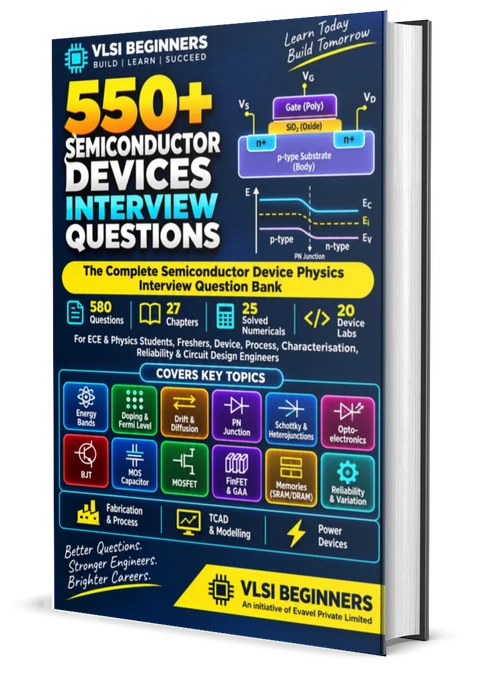
550+ Semiconductor Devices Interview Questions ebook cover
SEMICONDUCTOR DEVICES EBOOK · 580 QUESTIONS · 27 CHAPTERS

Get the complete device-physics question bank, fully answered

580 questions with interview-ready answers and tips, 20 Python and SPICE device labs, 25 solved numericals and 30 fab and lab debugging scenarios.

INSTANT PDF DOWNLOAD · 8 FREE PREVIEW PAGES
See the ebook

Semiconductor device questions check whether you understand what's physically happening inside a transistor or diode. They make up most of the interview for device, process, TCAD, characterisation and reliability roles, and they come up in circuit and memory interviews whenever leakage, breakdown or ageing is on the table.

The best answers start with a picture (a band diagram, a carrier flow, a depletion region) and only then bring in the equation. Begin with the formula sheet and the calculator, skim the 50 questions by topic, then attempt each worked answer and numerical before opening it.

HOW IT'S ASKED

Three levels of a device-physics interview

LEVEL 1

Carriers & bands

Bandgaps, the Fermi level, intrinsic and doped silicon, the mass-action law, drift and diffusion. Expect to draw a band diagram and place the Fermi level.

LEVEL 2

Junctions & transistors

The PN junction under bias, the diode equation, breakdown, Schottky contacts, BJT action, the MOS capacitor, threshold voltage and short-channel effects.

LEVEL 3

Real devices & real data

FinFET and GAA, power and wide-bandgap devices, reliability mechanisms, process steps, C–V and Hall measurements, and "this lot came out wrong; why?"

HOW TO ANSWER

Six habits of strong device-physics answers

01

Draw the band diagram first

Almost every junction, contact and MOS question becomes simple once Ec, Ev and EF are on the board. Interviewers often ask for it anyway.

02

Keep EF flat in equilibrium

No current means no Fermi-level gradient. This one rule fixes the shape of every equilibrium band diagram you'll draw.

03

Say which carrier, and where

Majority or minority? Drift or diffusion? Depletion region or neutral region? Diode current, for example, is minority-carrier diffusion in the neutral regions.

04

Quote one number

kT/q = 25.9 mV, ni ≈ 1010 cm−3, 60 mV per decade, Eg = 1.12 eV. A real number shows you can use the physics, not just describe it.

05

Use temperature as a clue

Positive or negative coefficient, activation energy near Eg or Eg/2: temperature behaviour separates mechanisms faster than anything else.

06

Link physics to the product

Bandgap to leakage and breakdown, mobility to drive current, traps to reliability. Show why the physics matters to a circuit or a fab.

FORMULA SHEET

The device equations interviewers expect

Silicon at 300 K unless stated: kT/q = 25.9 mV, ni ≈ 1×1010 cm−3, εSi = 11.7ε0, εox = 3.9ε0.

MASS ACTIONn·p = ni2 · n ≈ ND (n-type), p ≈ NA (p-type)
FERMI LEVELEF − Ei = kT·ln(n/ni) · Ei − EF = kT·ln(p/ni)
INTRINSIC nini ∝ T3/2·e−Eg/2kTRoughly doubles every 8–10 °C near room temperature in silicon.
CONDUCTIVITYσ = q(nμn + pμp) · ρ = 1/σ · Rs = ρ/t
EINSTEIND/μ = kT/q · diffusion length L = √(Dτ)
BUILT-IN POTENTIALVbi = (kT/q)·ln(NAND/ni2)
DEPLETION WIDTHW = √(2εs(Vbi + VR)/q · (1/NA + 1/ND))Most of W lies on the lightly doped side.
DIODEI = IS(eqV/nkT − 1) · ~60 mV per decade at n = 1, 300 K
THRESHOLDVT = VFB + 2φF + √(2qεsNA·2φF)/Cox · Cox = εox/tox
SUBTHRESHOLDS = 2.3·(kT/q)·(1 + Cdep/Cox) ≥ 60 mV/decade
HIGH-kEOT = tphys·(3.9/k)
HALLVH = IB/(qnt) · sign of VH gives the carrier type
TRY IT

Silicon carrier & Fermi-level calculator

Enter the doping and temperature. Uses ni(300 K) = 1×1010 cm−3, a temperature-dependent bandgap and a standard mobility model. Estimates, not a TCAD result.

ni AT THIS T–
TYPE–
ELECTRONS n–
HOLES p–
EF − Ei–
RESISTIVITY–


MATERIALS AT A GLANCE

Why silicon, and when not silicon?

"Why is GaN used for chargers?" or "why not make CPUs from GaAs?" both come down to these properties. Values are typical room-temperature figures.

MATERIALBANDGAP (eV)TYPEELECTRON MOBILITY (cm²/V·s)BREAKDOWN FIELD (MV/cm)WHERE IT WINS
Silicon1.12Indirect~1,400~0.3Logic, memory, most analog; cheap, great native oxide
Germanium0.66Indirect~3,900~0.1High hole mobility; SiGe strain and HBTs, IR detectors
GaAs1.42Direct~8,500~0.4RF front ends, lasers, high-efficiency solar
4H-SiC3.26Indirect~900~2.5–3High-voltage power: EV inverters, chargers, grid
GaN3.4Direct~1,000 bulk, ~2,000 in a HEMT channel~3.3Fast power switching, RF power, blue and white LEDs
BROWSE BY TOPIC

50 semiconductor interview questions across 10 topics

A sample of what device interviewers ask most. The 580-question ebook goes much deeper on each topic and answers every question.

Crystals & Energy Bands

Why semiconductors behave as they do.

  • What separates a metal, a semiconductor and an insulator in band terms?
  • Why does the bandgap shrink as temperature rises?
  • What is effective mass, and why is it different for electrons and holes?
  • What is a hole, physically?
  • Why is silicon's bandgap called indirect, and what does that change?

Doping & Carrier Statistics

Controlling how many carriers there are.

  • What happens to n, p and EF when you add donors?
  • What is the freeze-out region, and when does it matter?
  • What is a compensated semiconductor?
  • Why does a semiconductor become intrinsic again at high temperature?
  • When does the Boltzmann approximation fail?

Transport & Recombination

How carriers move and disappear.

  • Explain drift and diffusion current with an example of each.
  • Why does mobility fall with doping and with temperature?
  • What is velocity saturation?
  • Compare SRH, radiative and Auger recombination.
  • What is minority-carrier lifetime, and how is it measured?

PN Junctions & Diodes

The structure under almost every device.

  • How does the depletion region form, and what sets its width?
  • Why is diode current mostly minority-carrier diffusion?
  • What sets the ideality factor between 1 and 2?
  • Depletion versus diffusion capacitance: when does each dominate?
  • What limits a diode's switching speed?

Contacts & Optoelectronics

Metal junctions and light.

  • What decides whether a metal contact is ohmic or Schottky?
  • Why is a Schottky diode faster than a PN diode?
  • How does an LED generate light, and why not in silicon?
  • How does a solar cell produce power? Explain Voc, Jsc and fill factor.
  • What is a heterojunction, and where is it used?

Bipolar Transistors

Still asked, especially in analog.

  • Explain transistor action in an NPN BJT.
  • Why is the emitter heavily doped and the base thin?
  • What is the Early effect?
  • Why does current gain fall at low and high current?
  • What does a Gummel plot show?

MOS Capacitor & MOSFET

The heart of every chip.

  • Describe accumulation, depletion and inversion with band diagrams.
  • Why do low- and high-frequency C–V curves differ in inversion?
  • Which knobs set the threshold voltage?
  • What is the body effect?
  • Why did high-k dielectrics and metal gates replace SiO2 and poly?

Short-Channel & Advanced Devices

What changed as transistors shrank.

  • Explain DIBL and VT roll-off.
  • What is punch-through, and how do halo implants help?
  • What advantages does SOI offer, and what are its problems?
  • Why are FinFETs and nanosheets better at controlling the channel?
  • How does a GaN HEMT form its channel without doping?

Power, Memory & Reliability

Devices under stress.

  • How does an IGBT combine MOSFET and BJT behaviour?
  • How does a flash cell store charge, and why does it wear out?
  • Explain NBTI and how it recovers.
  • What is TDDB, and why are Weibull plots used?
  • What causes electromigration?

Fabrication & Characterisation

Making and measuring devices.

  • Thermal oxidation: why is wet faster than dry?
  • Why is an anneal needed after ion implantation?
  • How does a four-point probe remove contact resistance?
  • How is doping extracted from a C–V measurement?
  • What is TCAD, and how does it differ from a compact model?

These are samples. The full bank is six times larger.

580 questions in 27 chapters, all answered: 20 Python and SPICE device labs, 25 solved numericals, 30 debugging scenarios, plus optoelectronics, power devices, memories, process and TCAD.

See the full question bank
N1 · CARRIER DENSITIESBEGINNERSilicon is doped with 5×1016 cm−3 donors. Find n and p.Show solution ↓
N_D ≫ n_i → n ≈ N_D = 5 × 10^16 cm^-3
p = n_i² / n = 10^20 / (5 × 10^16) = 2 × 10^3 cm^-3

Note: fourteen orders of magnitude between majority and minority carriers.

N2 · FERMI LEVELBEGINNERFor the same sample, how far above Ei is the Fermi level?Show solution ↓
E_F − E_i = kT·ln(n/n_i)
          = 0.0259 × ln(5 × 10^6)
          = 0.0259 × 15.42 ≈ 0.40 eV

Note: with Ec about 0.56 eV above Ei, EF sits roughly 0.16 eV below the conduction band.

N3 · RESISTIVITYBEGINNERn-type silicon with ND = 1016 cm−3 and μn = 1,350 cm2/V·s. Find the resistivity.Show solution ↓
ρ = 1 / (q·n·µ_n)
  = 1 / (1.6 × 10^-19 × 10^16 × 1350)
  = 1 / 2.16 ≈ 0.46 Ω·cm

Note: holes contribute nothing measurable here; p is only 104 cm−3.

N4 · BUILT-IN POTENTIALINTERMEDIATEA PN junction has NA = 1017 and ND = 1016 cm−3. Find Vbi.Show solution ↓
V_bi = (kT/q)·ln(N_A·N_D / n_i²)
     = 0.0259 × ln(10^33 / 10^20)
     = 0.0259 × ln(10^13) = 0.0259 × 29.93 ≈ 0.78 V

Note: Vbi grows only logarithmically, which is why it stays between about 0.6 and 1.0 V for silicon.

N5 · DEPLETION WIDTHINTERMEDIATEA one-sided p+n junction has ND = 1016 cm−3 and Vbi = 0.8 V. Find the depletion width at 5 V reverse bias (εs = 1.04×10⁻¹² F/cm).Show solution ↓
W = √(2·ε_s·(V_bi + V_R) / (q·N_D))
  = √(2 × 1.04e-12 × 5.8 / (1.6e-19 × 1e16))
  = √(7.5 × 10^-9 cm²) ≈ 8.7 × 10^-5 cm ≈ 0.87 µm

Note: almost all of it is on the lightly doped n side.

N6 · DIODE VOLTAGEBEGINNERAn ideal diode carries 1 mA at 0.60 V. What voltage gives 10 mA? And if the ideality factor were 1.5?Show solution ↓
ΔV = n·(kT/q)·ln(10)
n = 1   : ΔV = 0.0259 × 2.303 ≈ 60 mV → 0.66 V
n = 1.5 : ΔV ≈ 89 mV              → 0.69 V

Note: measuring the slope per decade is the quickest way to extract the ideality factor.

N7 · DIFFUSION LENGTHINTERMEDIATEMinority electrons have μn = 1,200 cm2/V·s and lifetime τ = 1 µs. Find Dn and Ln.Show solution ↓
D_n = (kT/q)·µ_n = 0.0259 × 1200 ≈ 31 cm²/s
L_n = √(D_n·τ) = √(31 × 10^-6) ≈ 5.6 × 10^-3 cm ≈ 56 µm

Note: a BJT base must be much thinner than this, and a solar cell should collect carriers from within about this distance of the junction.

N8 · OXIDE CAPACITANCE & EOTINTERMEDIATEFind Cox for 2 nm of SiO2. What is the EOT of 4 nm of HfO2 (k = 20)?Show solution ↓
C_ox = ε_ox / t_ox = (3.9 × 8.85e-14) / (2e-7 cm)
     ≈ 1.73 × 10^-6 F/cm² ≈ 17 fF/µm²
EOT  = 4 nm × 3.9 / 20 ≈ 0.78 nm

Note: high-k gives the capacitance of 0.78 nm of SiO2 with a physically thicker film, which cuts gate tunnelling leakage dramatically.

depletion region qVbi EcEiEvEF p-typen-type
Fermi level EFBand edgesDepletion region
  1. Draw each side on its own first. On the p side, EF sits just above Ev; on the n side, just below Ec. Both have the same bandgap.
  2. Make the Fermi level one flat line. In equilibrium there's no net current, so EF can't vary with position. Draw it straight across.
  3. Bend the bands to fit. Far from the junction each side keeps its own EF position. In between, Ec, Ei and Ev bend together by the same amount, which is qVbi.
  4. Mark the depletion region. All the bending happens there. It's wider on the lighter-doped side, and the field points from the n side to the p side.
  5. Read the barrier. Electrons on the n side must climb qVbi to reach the p side. Forward bias lowers that barrier by qV; reverse bias raises it.
Why must the Fermi level be flat in equilibrium?

The net electron current is proportional to n·μn·dEF/dx, and similarly for holes. With no current flowing, the gradient of EF must be zero everywhere. A sloped Fermi level always means current is flowing.

What sets the amount of band bending?

The difference between the two Fermi levels before contact: qVbi = kT·ln(NAND/ni2). For NA = 1017 and ND = 1016 cm−3 that is about 0.78 eV, as in numerical N4 above.

What changes under forward and reverse bias?

The Fermi level splits into two quasi-Fermi levels, one for electrons and one for holes, separated by qV across the depletion region. Forward bias reduces the bending to q(Vbi − V) and narrows the depletion region; reverse bias increases it to q(Vbi + VR) and widens it.

How does a Schottky contact's diagram differ?

One side is a metal, so its bands don't bend and all the bending happens in the semiconductor. The barrier seen from the metal side, ΦB, is fixed by the interface rather than by doping. That's why Schottky diodes have a lower turn-on voltage and no minority-carrier storage. The ebook has full chapters on junction electrostatics and metal–semiconductor contacts.

Bandgap of silicon at 300 K?

1.12 eV.

Thermal voltage kT/q at 300 K?

About 25.9 mV.

Intrinsic carrier density of silicon at 300 K?

About 1010 cm−3 (modern value ≈ 9.7×10⁹).

The mass-action law?

n·p = ni2 in equilibrium.

The Einstein relation?

D/μ = kT/q.

Faster carrier in silicon?

Electrons.

Is silicon's bandgap direct or indirect?

Indirect.

Ideal diode current change per 60 mV at 300 K?

Ten times.

Temperature coefficient of avalanche breakdown?

Positive.

Where is EF in n-type silicon?

Near the conduction band.

Dominant capacitance in forward bias?

Diffusion capacitance.

How is an ohmic contact usually made?

Heavy doping, so carriers tunnel through a thin barrier.

Why a thin BJT base?

Less recombination, so higher gain and speed.

MOS-C capacitance in inversion at high frequency?

The minimum, Cmin.

Does reverse body bias raise or lower VT?

Raises it.

What does DIBL lower?

VT, as VDS rises.

Ideal subthreshold swing at 300 K?

About 60 mV/decade.

What forms the channel in a GaN HEMT?

A 2DEG from polarisation charge at the AlGaN/GaN interface.

Which transistor does NBTI mainly affect?

PMOS.

What does the sign of the Hall voltage tell you?

The majority carrier type.

COMMON MISTAKES

What costs candidates the most in device rounds

×

A sloping Fermi level in equilibrium

If nothing is biased, EF is flat. Drawing it bent across a junction is the single most common band-diagram error.

×

Forgetting the minority carriers

Diode, BJT and solar-cell currents are set by minority carriers diffusing. Answers that talk only about majority carriers miss the mechanism.

×

Equations with no physical picture

Interviewers want to hear what's happening first: a barrier lowering, a depletion region widening, carriers being swept or diffusing.

×

Ignoring temperature

ni, leakage, mobility, breakdown and reliability all depend strongly on it. Many scenario questions are solved by asking what happens when it's hot.

×

Mixing up Zener and avalanche

Different doping, different voltage, opposite temperature coefficients. Get all three right.

×

Units and orders of magnitude

cm versus m, cm−3 versus m−3. Quote typical values (1010, 1016, 1,400) so the interviewer can see your numbers are sane.

QUICK FAQ

Before you start preparing

Which jobs ask semiconductor device questions?

Device, process integration, TCAD, characterisation, reliability and yield roles test device physics in depth. Circuit, memory and analog design interviews ask the basics, and most core-company written tests for ECE graduates include them.

How much maths is expected?

Mostly order-of-magnitude calculations: carrier densities, Fermi-level position, built-in potential, depletion width, diode current and threshold voltage. Interviewers care more about the physical picture and the right assumptions than about long derivations.

Which topics should a fresher prepare first?

Energy bands and the Fermi level, doping and the mass-action law, drift and diffusion, the PN junction band diagram and diode equation, breakdown, the MOS capacitor and MOSFET threshold voltage, and why short-channel effects led to FinFETs.

Do I need to know fabrication?

For process and device roles, yes: oxidation, lithography, etch, implantation, annealing, deposition and CMP, and how each affects device parameters. For design roles, knowing the main steps and why they matter is usually enough.

Are wide-bandgap and power devices asked?

Increasingly, yes, especially at power-electronics, automotive and compound-semiconductor companies. Know why SiC and GaN suit high voltage and high frequency, how a HEMT forms its channel, and how IGBTs and superjunction MOSFETs work.

How is this different from the CMOS round?

This round is about how devices work inside: bands, carriers, junctions and transistor physics. The CMOS round uses those devices to build circuits, and asks about sizing, delay, power and memory cells.

Want to be tested on these live?

Book a 1:1 mock interview with a mentor working in this exact domain.

Book a mock interview