SEMICONDUCTOR INTERVIEW PREP

Walk into your next chip design interview actually ready.

Free interview question banks, mentor-led mock interviews, and structured workshops across Verilog, SystemVerilog, RTL, FPGA, ASIC, Physical Design, STA and DFT — built with real semiconductor industry mentors.

18
VLSI DOMAINS
15,000+
INTERVIEW QUESTIONS
1:1
MOCK INTERVIEWS
FREE
QUESTION BANKS
INSIDE A CHIP

Here's what's actually inside the thing you're interviewing about

Pop the lid off any packaged chip and this is roughly what you'd find. Every domain we cover — RTL, Physical Design, DFT — maps to one of these physical parts.

Package lid

The metal or ceramic cap that seals everything inside — this is the part you're watching lift open.

Bond wires

Hair-thin gold or copper wires carrying every signal off the die to the package leads.

WATCH THE LID — IT OPENS ON A LOOP
Silicon die

The actual chip — billions of transistors packed into a few millimetres of silicon.

Leadframe & pins

Where the package finally connects outward — onto the circuit board.

FROM IDEA TO SILICON

The chip design flow, in ten stages

Every VLSI job owns one or two of these stages. Click through to see what happens in each, who does it, and what interviewers ask about it.

STAGE 01 OF 10

Specification and architecture

Architects turn product goals into numbers: performance, power, area and cost. They then split the chip into blocks and decide the micro-architecture: pipelines, memories, buses and clock domains.

WHO DOES IT
Architects and senior designers
WHAT COMES OUT
Specification and micro-architecture documents
AN INTERVIEWER MIGHT ASK

“How would you size a FIFO between a fast writer and a slow reader?”

ASIC design questions →
STAGE 02 OF 10

RTL design

Designers describe the hardware in Verilog or SystemVerilog at the register-transfer level: registers, the logic between them, state machines and interfaces. The code is linted and checked for clock-domain crossings before anyone else uses it.

WHO DOES IT
RTL / ASIC design engineers
WHAT COMES OUT
Synthesizable RTL, lint- and CDC-clean
AN INTERVIEWER MIGHT ASK

“What's the difference between blocking and non-blocking assignments, and why does it matter in a flip-flop?”

RTL design questions →
STAGE 03 OF 10

Functional verification

Usually the largest team on a chip. Engineers build SystemVerilog/UVM testbenches, generate constrained-random stimulus, write assertions and measure coverage until they're confident the RTL matches the spec. Formal tools prove some properties mathematically.

WHO DOES IT
Design verification (DV) engineers
WHAT COMES OUT
Passing regressions and coverage closure
AN INTERVIEWER MIGHT ASK

“What's the difference between code coverage and functional coverage?”

UVM questions →
STAGE 04 OF 10

Logic synthesis

A synthesis tool maps the RTL onto real standard cells from the foundry's library, guided by timing constraints written in SDC: clocks, input/output delays, false and multicycle paths.

WHO DOES IT
RTL and implementation engineers
WHAT COMES OUT
Gate-level netlist and constraints
AN INTERVIEWER MIGHT ASK

“What does a false-path constraint tell the tool, and when is it dangerous?”

STA questions →
STAGE 05 OF 10

Design for test

Flip-flops are stitched into scan chains, memories get built-in self-test, and ATPG generates test patterns, so that every manufactured chip can be checked for defects in seconds.

WHO DOES IT
DFT engineers
WHAT COMES OUT
Scan-inserted netlist and test patterns
AN INTERVIEWER MIGHT ASK

“Why do we need scan chains, and what is stuck-at fault coverage?”

DFT questions →
STAGE 06 OF 10

Floorplan and placement

Physical designers decide the die size, place large blocks (macros) and I/O, build the power grid, then place millions of standard cells while watching congestion and timing.

WHO DOES IT
Physical design engineers
WHAT COMES OUT
Placed design with a power grid
AN INTERVIEWER MIGHT ASK

“Why do we leave halos around macros?”

Physical design questions →
STAGE 07 OF 10

Clock tree synthesis and routing

The clock is distributed through a balanced tree of buffers so it arrives at every flop at nearly the same time. Then the router connects every net across ten or more metal layers without breaking design rules.

WHO DOES IT
Physical design engineers
WHAT COMES OUT
Routed, DRC-clean layout
AN INTERVIEWER MIGHT ASK

“What is clock skew, and when is useful skew actually helpful?”

Physical design questions →
STAGE 08 OF 10

Sign-off: timing, power and physical checks

Static timing analysis checks every path across process, voltage and temperature corners. Engineers also verify IR drop, electromigration and power, and run DRC and LVS to prove the layout matches the netlist and the foundry's rules.

WHO DOES IT
STA, PD and sign-off engineers
WHAT COMES OUT
Clean timing, power and physical reports
AN INTERVIEWER MIGHT ASK

“What is on-chip variation, and why do we apply derates?”

STA questions →
STAGE 09 OF 10

Tape-out and fabrication

The final layout (GDSII or OASIS) goes to the foundry. Masks are made and wafers spend roughly three months moving through hundreds of process steps before finished dies come out.

WHO DOES IT
Whole team; foundry process engineers
WHAT COMES OUT
Wafers of finished dies
AN INTERVIEWER MIGHT ASK

“What happens between tape-out and first silicon?”

What's inside a chip →
STAGE 10 OF 10

Test, bring-up and validation

Packaged parts are tested on automatic test equipment, then validation engineers bring the chip up on boards, run real software and characterise it across voltage and temperature. Bugs found here lead to fixes or a re-spin.

WHO DOES IT
Test, product and post-silicon validation engineers
WHAT COMES OUT
Production-qualified chip
AN INTERVIEWER MIGHT ASK

“How would you debug a chip that fails only at high temperature?”

Semiconductor questions →
EVERY CAREER STAGE

Built for wherever you are right now

The prep that helps a final-year student is not the prep that helps someone switching from DV to Physical Design. We structure content around where you actually are.

STUDENTS

Build the foundation

Get digital electronics, Verilog, and core VLSI concepts solid before your first campus interview.

FRESHERS

Turn knowledge into answers

Structured question banks plus a live mock interview to convert what you've studied into confident, interview-ready responses.

WORKING PROFESSIONALS

Sharpen a specific gap

STA, DFT, UVM, Physical Design — work with a mentor who's in that exact domain day to day, not a generalist.

JOB SWITCHERS

Move between sub-domains

Moving from DV to Physical Design, or RTL to DFT? Get targeted prep and honest feedback on where you actually stand.

CHOOSE A TRACK

Six VLSI career tracks, in plain language

"VLSI" isn't one job — it's a set of very different day-to-day roles. Here's what each one actually involves, so you can target your prep instead of studying everything at once.

RTL / DIGITAL DESIGN

Write the logic that becomes the chip

You describe hardware behavior in Verilog/SystemVerilog — datapaths, FSMs, pipelines — that RTL-to-GDS tools later turn into silicon.

Core skills: Verilog, SystemVerilog, microarchitecture, timing basics
RTL interview questions →
DESIGN VERIFICATION

Prove the design does what it should

You build testbenches and constrained-random environments to catch bugs before tape-out — often the largest team on a chip project.

Core skills: SystemVerilog, UVM, assertions, coverage-driven verification
UVM interview questions →
PHYSICAL DESIGN

Turn logic into physical silicon

You take the verified netlist through floorplanning, placement, clock-tree synthesis, and routing until it meets timing, power, and area targets.

Core skills: STA, floorplanning, CTS, place & route tools
Physical Design questions →
DFT

Make sure every chip can be tested

You insert scan chains, BIST, and boundary scan so manufactured chips can be tested for defects cheaply and thoroughly on the tester floor.

Core skills: scan insertion, ATPG, BIST, fault models
DFT interview questions →
ANALOG / MIXED-SIGNAL

Design the parts that aren't purely digital

You design amplifiers, PLLs, ADCs/DACs, and I/O — the circuits that touch the real, continuous world rather than clean 1s and 0s.

Core skills: transistor-level design, SPICE simulation, layout awareness
Analog VLSI questions →
EMBEDDED SYSTEMS

Bring the chip to life with software

You write firmware and drivers that run directly on the hardware — the layer that sits closest to silicon, above pure chip design.

Core skills: C/C++, microcontrollers, RTOS, hardware/software interfaces
Embedded systems questions →
CAREERS, BY THE NUMBERS

What the job market actually looks like

Researched pay, the internship calendar and where the jobs cluster. Each card opens a full guide.

INDIA INTERNSHIP CALENDAR
  • JUL – NOVCampus intern drives for pre-final-year B.Tech
  • SEP – NOVAbroad research programs close (Mitacs, DAAD WISE)
  • DEC – FEBM.Tech long internships allocated
  • MAY – JULSummer internships run; PPOs follow
Programs and stipends →
WORLDWIDE

Wherever you're planning to study, we've mapped it

Universities, private training institutes, and government-backed programs across 10 countries — so you know what actually exists before you pick a course.

10
COUNTRIES
99
PROGRAMS
Browse institutes worldwide →
India
USA
Taiwan
South Korea
Germany
UK
Singapore
Japan
China
Netherlands
WHO'S HIRING

Know exactly who's hiring, and where to apply

Foundries, global design centers, EDA vendors, and equipment makers — mapped country by country, with a direct link to each company's own careers page instead of a generic job board.

11
COUNTRIES LIVE
159
COMPANIES
Browse companies worldwide →
THREE WAYS IN

No fixed sequence — start wherever you are

Browse free content, buy a focused ebook, or go straight to a mentor. Each path stands on its own.

LEARN — FREE

Interview question banks

Foundational, applied, and scenario/debug level questions across every core VLSI domain, filterable by topic and depth.

Browse questions →
EBOOKS — PAID

Structured ebooks

Questions-only prep sets — SystemVerilog, RTL Design, UVM, and more — for focused, offline revision before your interview.

See ebooks →
MENTORSHIP — PAID

Mock interviews & workshops

1:1 mock interviews and live workshops with working semiconductor professionals, with honest, direct feedback.

Book a mentor →
WHY VLSI, RIGHT NOW

The industry behind the interview

Semiconductor demand isn't a talking point — it's the reason this prep matters right now.

$1T+
GLOBAL SEMICONDUCTOR INDUSTRY REVENUE, 2026 — A RECORD HIGH
AI + HBM
AI ACCELERATORS AND HIGH-BANDWIDTH MEMORY ARE THE BIGGEST DEMAND DRIVERS TODAY
6
CORE CAREER TRACKS — RTL, VERIFICATION, PHYSICAL DESIGN, DFT, ANALOG, AND EMBEDDED
GLOBAL
DEMAND ACROSS US, EUROPE, AND ASIA PACIFIC FABS AND DESIGN CENTERS

Figures reflect broad 2026 industry forecasts (WSTS, Gartner, Deloitte) and are directional, not a guarantee of any individual outcome.

INDIA, 2026

India started making chips this year

Under the India Semiconductor Mission, 12 projects are approved and four assembly-and-test plants began production in 2026. That creates a new kind of VLSI job in India: test, product, packaging and process engineering.

  • 12ISM projects approved
  • 4plants in production
  • 2028first commercial fab targeted
See every Indian employer →
India Semiconductor Mission plants, status in October 2026
COMPANYWHERETYPESTATUS
MicronSanand, GujaratMemory assembly and test (ATMP)In productionSince Feb 2026
Kaynes SemiconSanand, GujaratOSATIn productionSince Mar 2026
CG SemiSanand, GujaratOSATIn productionSince Jul 2026
Suchi SemiconSurat, GujaratOSATIn productionSince Sep 2026
Tata ElectronicsJagiroad, AssamAssembly and testUnder construction
HCL–FoxconnJewar, Uttar PradeshOSATUnder construction
Tata Electronics + PSMCDholera, Gujarat300 mm wafer fabPlannedTarget: 2028

Status as reported by government and press sources, October 2026.

FROM SAND TO SILICON

How a chip actually gets made

The interview questions make more sense once you can picture the physical process behind them.

Silicon Wafer

A thin slice of ultra-pure crystalline silicon — the base material every chip starts as.

Photolithography

UV light projects the circuit pattern onto a photosensitive layer coating the wafer.

Etching & Doping

Unwanted material is etched away layer by layer; dopants are added to create transistor regions.

Packaging

The die is cut, mounted, and enclosed in a package with pins connecting it to a circuit board.

Testing (DFT)

Every chip is tested against fault models before it ships — this is where DFT engineers do their work.

READ THE WAVEFORM

If you can't read this diagram, the interview gets hard fast

Setup and hold time is asked in almost every digital and STA interview — and almost always as a diagram like this one, not a definition.

CLK DATA Tsu Th CAPTURE EDGE

CLK is the clock — the capture edge (dashed line) is the instant a flip-flop actually samples its input.

DATA has to be stable for Tsu (setup time) before that edge, and stay stable for Th (hold time) after it — miss either window and the flip-flop can sample garbage.

We wrote a full breakdown of how to explain this — and the fixes for each type of violation — the way interviewers are actually listening for it.

Read the full explanation →
QUICK REFERENCE

Twelve numbers every VLSI engineer should know

Interviewers drop these into questions and expect you to know them without looking. Each card links to the topic behind it.

300 mmWafer diameterThe standard wafer size at modern fabs. A bigger wafer holds more dies, so each chip costs less.13.5 nmEUV wavelengthExtreme-ultraviolet lithography uses 13.5 nm light to print the finest layers, versus 193 nm for older DUV tools.4Transistors in a NAND2Two PMOS in parallel, two NMOS in series. Interviewers love asking you to draw it.6TSRAM bit cellSix transistors store one bit in SRAM: two cross-coupled inverters plus two access transistors. DRAM uses 1T1C.αCV²fDynamic powerPower grows with the square of voltage, so lowering the supply is the strongest power lever.2 flopsMinimum synchronizerA single-bit signal crossing clock domains needs at least two flip-flops to give metastability time to resolve.T ≥ tcq + tlogic + tsuSetup checkData launched on one edge must arrive a setup time before the next edge. Clock skew adds or subtracts.tcq + tlogic ≥ thHold checkData must not change too soon after the same edge. The clock period doesn't appear, so slowing the clock can't fix hold.PVTCornersProcess, voltage and temperature. Timing must close at the slow and fast extremes, not just typical.10+Metal layersAdvanced chips stack ten or more copper wiring layers, thin ones for local signals and thick ones for power and clocks.2ⁿStates in n flopsA binary counter uses all 2ⁿ states; one-hot uses n flops for n states but decodes faster; Gray code changes one bit at a time.208 billionTransistors in one GPUNVIDIA's Blackwell GPU packs 208 billion transistors across two dies, one of the largest chips ever made.
SPEAK THE LANGUAGE

Eight terms every interviewer assumes you know

Not definitions to memorize — the actual working meaning, the way it comes up mid-interview.

Setup & Hold Time
The window before/after a clock edge that data must stay stable so a flip-flop samples it correctly.
Tape-out
The point a chip's final design is frozen and sent to the fab for manufacturing — no more changes after this.
Testbench
The verification environment that generates inputs, checks outputs, and measures coverage against the design under test.
Scan Chain
Flip-flops rewired in test mode into a shift register, so internal chip state can be read out and checked for defects.
Floorplanning
Deciding where major blocks, macros, and I/O physically sit on the die before detailed placement and routing.
CMOS
The transistor technology — paired NMOS/PMOS switches — that essentially every modern digital chip is built from.
RTL
Register-Transfer Level — hardware described as data moving between registers each clock cycle, the level Verilog/SV code sits at.
Yield
The percentage of chips on a wafer that pass testing and work correctly — a core economic metric for any fab.

Browse the full study notes & glossary →

FREE QUESTION BANKS

All 18 domains, one interview roadmap

Every domain has its own free question bank, from fundamentals up to debug-level scenarios. Banks marked EBOOK also have a full question set you can download. When you're ready, the last two cards test you the way an interview would.

Prefer to browse and filter by depth level? Visit the full interview questions hub →

Prefer to study before you test yourself? Visit the Learn Hub →

FREE STUDY TOOLKIT

Everything you need before the question bank

Free references for building the fundamentals, whichever way you learn best.

Open the Learn Hub →
CAREER TOOLS

From first application to signed offer

Salaries, company interview guides, fresher job sources and a resume method, all free.

See pricing →
GO DEEPER

Ebooks for offline revision

Fifteen ebooks, each with a free preview before you buy. Here are the six newest, all fully answered; the other nine (CDC, FPGA, DFT, STA, SystemVerilog, Physical Design, UVM, RTL Design and General VLSI) are on the ebooks page. Eleven of the fifteen include full answers.

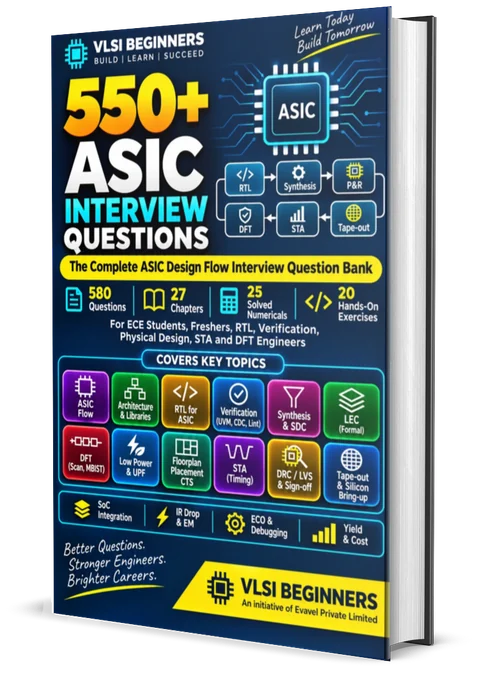
NEWASIC Design Interview Questions ebook cover

ASIC Design

580 questions, with answers
Learn more →
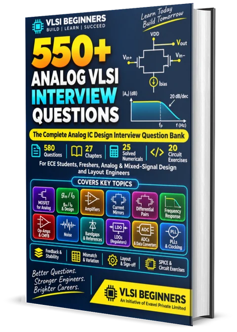
NEWAnalog VLSI Interview Questions ebook cover

Analog VLSI

580 questions, with answers
Learn more →
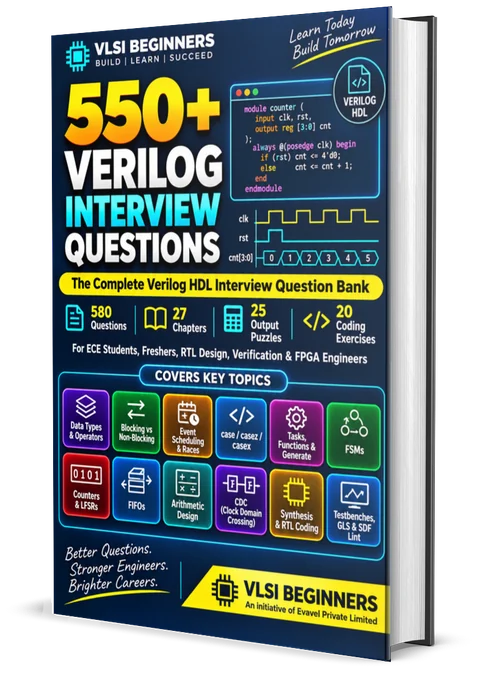
NEWVerilog Interview Questions ebook cover

Verilog

580 questions, with answers
Learn more →
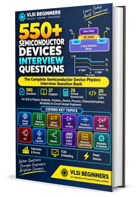
Semiconductor Devices Interview Questions ebook cover

Semiconductor Devices

580 questions, with answers
Learn more →
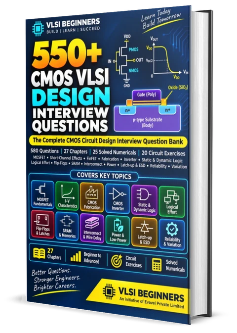
CMOS Interview Questions ebook cover

CMOS

580 questions, with answers
Learn more →
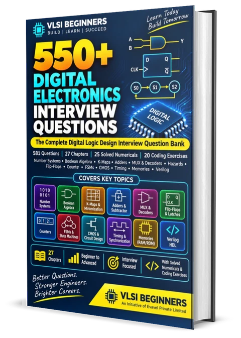
Digital Electronics Interview Questions ebook cover

Digital Electronics

581 questions, with answers
Learn more →

See all 15 ebooks →

SAMPLE

Real questions, not trivia

Every bank is written at three depth levels — foundational, applied, and scenario/debug — the way interviewers actually probe.

See the full bank
// RTL Design — Scenario/Debug
Q. Your synchronous FIFO shows
   data corruption only under
   back-to-back writes near full.
   Where do you start debugging,
   and why?

// SystemVerilog — Applied
Q. When would you use a
   virtual interface over a
   direct interface handle
   in a testbench?
TRY ONE NOW

Answer it out loud before you peek

Six real interview questions across domains, with a new set every day. Say your answer first, then open the hint or see what a strong answer covers.

TODAY · 6 QUESTIONS6 PRACTICE QUESTIONS
STA · FOUNDATIONAL

A flip-flop has a clock-to-Q delay of 0.3 ns and a setup time of 0.2 ns. The logic between it and the next flop takes 3.1 ns. Ignoring clock skew, what is the maximum clock frequency?

Hint

Data launched on one edge has to arrive, and be stable for the setup window, before the next edge.

What a strong answer covers
  • Tclk ≥ Tclk-q + Tlogic + Tsetup = 0.3 + 3.1 + 0.2 = 3.6 ns, so fmax ≈ 278 MHz.
  • Where skew fits in: positive skew at the capture flop relaxes setup; negative skew tightens it.
  • Hold is checked separately, and changing the clock frequency does not fix it.
More STA questions →
VERILOG · APPLIED

Inside always @(posedge clk), what hardware do you get from b = a; c = b; compared with b <= a; c <= b;?

Hint

Think about which value of b the second statement reads in each case.

What a strong answer covers
  • Blocking: c reads the new b, so both registers load a on the same edge. There's no pipeline stage between them.
  • Non-blocking: every right-hand side is sampled before any update, so c gets the old b. That's a two-stage shift register.
  • The rule behind it: non-blocking for sequential logic, blocking for combinational logic. This avoids simulation races and simulation/synthesis mismatches.
More Verilog questions →
RTL · CDC · SCENARIO / DEBUG

A one-cycle pulse crosses from a 100 MHz domain into a 25 MHz domain through a two-flop synchronizer, and the receiver sometimes misses it. Why? How would you fix it?

Hint

Compare the width of the pulse with the destination clock period.

What a strong answer covers
  • The pulse is 10 ns wide, but the destination samples only every 40 ns, so it can fall between two capture edges. A synchronizer handles metastability. It can't recover an event it never sampled.
  • Fix: convert the pulse into a toggle in the source domain, synchronize the level, then edge-detect it in the destination (a pulse synchronizer). Alternatively, use a req/ack handshake.
  • Bonus: stretching the pulse works only if you can guarantee a minimum spacing between pulses.
More RTL design questions →
UVM · FOUNDATIONAL

What is the difference between a UVM sequence and a UVM sequencer?

Hint

One of them is a uvm_object, and the other is a uvm_component.

What a strong answer covers
  • A sequence is a transient uvm_object that generates sequence items, which is the stimulus itself.
  • A sequencer is a uvm_component that lives in the testbench hierarchy. It arbitrates between running sequences and hands items to the driver through seq_item_port/seq_item_export.
  • Why it matters: keeping them separate lets you swap stimulus without touching the environment.
More UVM questions →
PHYSICAL DESIGN · SCENARIO / DEBUG

After CTS, setup timing is clean but dozens of short paths show hold violations. What are your options, and why won't slowing the clock help?

Hint

Look at whether the clock period appears anywhere in the hold equation.

What a strong answer covers
  • For same-edge paths, the hold check compares data arrival with the same clock edge, so the period drops out. A slower clock changes nothing.
  • Fixes: insert delay cells or buffers on the data path, swap to slower or higher-Vt cells, or rework skew on the offending clock branches.
  • Check that every hold fix leaves setup margin, and fix hold at the correct (fast) corner.
More physical design questions →
DFT · FOUNDATIONAL

What does the stuck-at fault model assume? Why is it still the baseline for manufacturing test when real defects are more varied?

Hint

Think about what makes a fault model useful for ATPG, even when it isn't physically exact.

What a strong answer covers
  • It assumes a single net is permanently tied to logic 0 or logic 1.
  • It's simple enough for ATPG to target efficiently and gives a clear coverage metric. Patterns that catch stuck-at faults also catch many real defects.
  • Its limits: it misses timing-related defects, which is why transition and path-delay fault models are added on top.
More DFT questions →
FROM THE BLOG

Latest interview prep & industry news

Fresh scenario-based prep articles and semiconductor hiring news, added regularly.

See all posts →
ARTICLE · INDUSTRY TRENDS

Agentic AI in Chip Design: What It Means for VLSI Freshers in 2026

AI agents can now draft RTL, generate testbenches and triage regressions. That doesn't end fresher hiring, but it does change what interviewers expect you to bring.

ARTICLE · CAREER GUIDE

Verification vs RTL Design vs Physical Design: Which VLSI Career Should You Choose?

Most freshers pick a VLSI track by accident. Here's what verification, RTL design and physical design actually involve, how their interviews differ, and a simple way to decide which one fits you.

NEWS · INDIA SEMICONDUCTOR MISSION

India Now Has Four Chip Plants in Production as Suchi Semicon Starts Up in Surat

With Suchi Semicon's Surat plant online, four India Semiconductor Mission units are now shipping chips in 2026. What's running, what comes next, and which jobs these plants create.

Semiconductor industry news only →

ON THE CALENDAR

Upcoming semiconductor events worth knowing

Interviewers notice when you follow the field. These are the events that matter for design, verification, and test roles.

11–16 OCT 2026

International Test Conference

SAN ANTONIO, USA

The premier chip-test and DFT conference. It's directly relevant if you're preparing for a DFT role.

8–12 NOV 2026

ICCAD 2026

SAN JOSE, USA

The top research venue for EDA, from synthesis algorithms to physical design tools.

17–18 NOV 2026

DVCon Europe

MUNICH, GERMANY

The design and verification conference, and the most relevant one for SystemVerilog and UVM interviews.

14–18 FEB 2027

ISSCC 2027

SAN FRANCISCO, USA

Often called the “Olympics of chip design,” and the top venue for circuit research worldwide.

Dates are taken from our hand-checked events calendar. Always confirm on the official event site before booking travel.

HOW IT WORKS

A simple, structured path to an offer

01

Learn

Start with free question banks across 18 VLSI domains — foundational, applied, and scenario levels.

02

Practice

Reinforce with a free live session, an ebook, or a full workshop — whichever matches how you learn.

03

Mock Interview

Get tested live by a working mentor and receive written, specific feedback within 48 hours.

04

Get Hired

Walk into the real interview having already been questioned the way a real panel questions.

MENTORS

Get interviewed by engineers who do this job

6 mentors across verification, design and implementation, each working in or recently from the semiconductor industry. Pick the one closest to the role you want.

Avnita

Design Verification Mentor
BEST FORFreshers and students moving into verification

Gets freshers ready for their first DV round, from SystemVerilog OOP to a working self-checking testbench.

See Avnita’s focus areas →

Sonia

UVM Verification Mentor
BEST FORVerification engineers with 1–5 years' experience

Runs UVM rounds built around your own testbench: sequences, factory, config_db, phasing and debug.

See Sonia’s focus areas →

Priyanka

SVA & Coverage Mentor
BEST FORDV candidates preparing for deep-dive rounds

Takes DV candidates deep into assertions, coverage planning and closing coverage holes.

See Priyanka’s focus areas →

Nitin

Synthesis, Low Power & STA Mentor
BEST FORFront-end and implementation roles where synthesis and timing are tested

Bridges RTL and layout: synthesis constraints, low-power design and fixing timing from real reports.

See Nitin’s focus areas →

Manoj

RTL & FPGA Mentor
BEST FORMid-to-senior engineers switching roles or companies

Pushes mid-to-senior designers on micro-architecture, FPGA timing and defending trade-offs.

See Manoj’s focus areas →

Ananya

Physical Design Mentor
BEST FORPhysical design and STA candidates, freshers to switchers

Builds PD rounds from real problems: floorplans, CTS, congestion, IR drop and corner-specific timing.

See Ananya’s focus areas →

Ready for an honest mock interview?

Book a 1:1 session with a working industry mentor and get direct, specific feedback — not generic tips.

Book a mock interview
MYTHS VS FACTS

Six things beginners believe about VLSI careers

Most bad career decisions in VLSI start with one of these. Tap a myth to see what actually happens in industry.

MYTHYou need an M.Tech to get a VLSI job.

FACTIt helps for RTL design and analog roles, but verification and physical design teams hire strong B.Tech graduates every year, especially those with internships and real projects.

MYTHA training-institute certificate gets you hired.

FACTEmployers hire what you can explain in an interview. Two projects you can defend line by line beat any certificate. Never pay for a "placement guarantee".

MYTHVerification is a lesser job than design.

FACTDV is usually the biggest team on a chip and pays in the same range as design. Many senior architects started in verification.

MYTHVLSI is just writing Verilog.

FACTCoding is one part. Timing, power, test, physical layout, debugging and communication matter as much, and that's what interviewers probe.

MYTHYou must be in Bengaluru to work in VLSI.

FACTBengaluru has the most jobs, but Hyderabad, Noida, Chennai, Pune and the new Gujarat plants all hire, and remote interviews are normal.

MYTHAnalog is dying because everything is digital.

FACTEvery chip needs power management, clocks, I/O and data converters. Experienced analog designers are among the hardest engineers to hire.

FAQ

Before you start

The questions people ask us most. See the full FAQ →

Do I need prior industry experience to start?

No. Our question banks and free resources are built for complete beginners and engineering students.

Can I prepare for free?

Yes — question banks, the free live session, and several downloads are free. Ebooks, workshops, and mock interviews are paid.

How is a mock interview different from reading a question bank?

A mock interview adapts to your answers in real time with follow-ups — see exactly how in our mock interview format guide.

What if I don't know which VLSI domain to specialize in?

Start with the General VLSI bank or the free live session — both are built to help you find your footing before committing to one domain.

Are the ebooks different from the free question banks?

Yes — the free banks are a sample across each domain. The ebooks package the complete set (500 to 1,500+ questions per domain) for focused, offline revision.

How do I book a mock interview or workshop?

Head to the booking page, pick a service, and choose a slot on our live calendar — confirmed instantly.

Is this only for freshers, or also for working professionals?

Both. Freshers get fundamentals-first prep, and working professionals get targeted mock interviews for the specific domain gap they're working on.

Do you cover company-specific interview prep?

Yes — our General VLSI ebook includes dedicated question sets for Intel, AMD, NVIDIA, Qualcomm, and more.