ASIC DESIGN FLOW INTERVIEW PREP

Spec to silicon, stage by stage. 580 ASIC questions, fully answered.

From architecture, libraries and RTL through verification, synthesis, SDC, equivalence checking, DFT and UPF to floorplanning, CTS, routing, STA, sign-off, tape-out and silicon bring-up, in 27 chapters. Each answer is written the way you'd say it in the interview, with a tip on what the interviewer will probe next. Includes 25 solved numericals, 20 hands-on exercises and 30 debugging scenarios.

181-PAGE PDF · INSTANT DOWNLOAD · 8 FREE PREVIEW PAGES BELOW
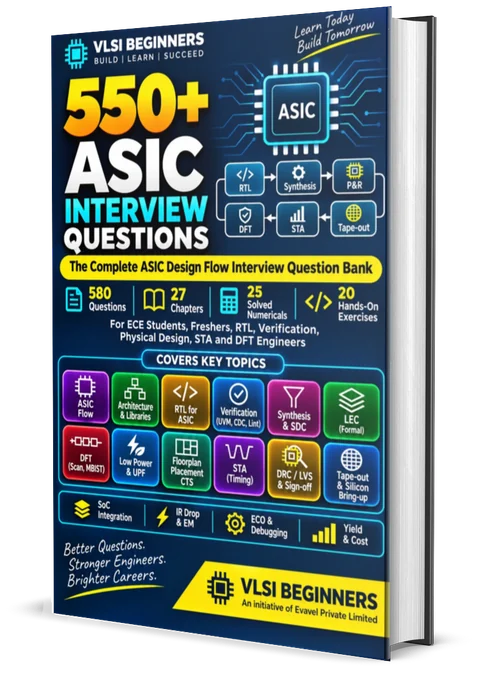
550+ ASIC Interview Questions ebook cover — VLSI Beginners
580
QUESTIONS WITH ANSWERS
27
CHAPTERS IN 5 PARTS
25
SOLVED NUMERICALS
20
HANDS-ON EXERCISES
THE PROBLEM

ASIC interviews test the whole flow, not just your stage of it

Every ASIC interview starts with “walk me through the flow”. Then it goes deep: what does synthesis need as input, what does a hand-off to physical design contain, how would you constrain this interface, why did hold break after routing?

A designer is asked about timing and DFT, and a physical design engineer about RTL and UPF. Interviewers want to see that you understand what happens before and after your own stage, can read a report, can do a quick calculation, and know what to do when timing still fails two weeks before tape-out.

This book follows a chip from specification to silicon: front-end design, then verification, synthesis and test, then low power and physical implementation, then sign-off, tape-out and bring-up, and finally the interview itself.

WHAT'S INSIDE

From the specification to a working chip

An ASIC round checks four things: do you know the flow and its hand-offs, can you reason about timing, power and test, can you calculate quickly, and can you make good decisions when something goes wrong late? Each has its own part of the book.

ANSWERS

580 answers, each with a tip

Questions are tagged Beginner, Intermediate or Advanced. Each gets a clear spoken-style answer and an Interview Tip: the term, number or follow-up that separates a good answer from a great one.

NUMERICALS

25 solved numericals

fmax, setup and hold slack, multicycle paths, OCV and CRPR, dynamic and leakage power, die sizing, IR drop, electromigration, crosstalk, clock trees, MTBF, FIFO depth, scan test time, dies per wafer, yield and ASIC versus FPGA cost.

HANDS-ON

20 exercises with verified results

Run with Yosys, Icarus Verilog and Python: latch inference, X in gate-level simulation, clock gating, FSM encoding, a small static timing analyser, OCV and POCV, repeaters, IR drop, a fault simulator, logic BIST and yield models.

DIAGRAMS

The pictures behind the flow

The standard-cell flow, a typical SoC, synthesis inputs and outputs, I/O delay budgets, scan chains, power domains, a block floorplan, the power grid, setup and hold checks, a clock tree and the yield-versus-area curve.

DEBUGGING

30 real debugging scenarios

2000 hold violations after routing, LEC failing after an ECO, an IR-drop hotspot, a chip that fails only when hot, X after reset in GLS, scan chain failures on the tester, mismatched SDCs and a late RTL fix before tape-out.

QUICK REVISION

Built for the last day

The flow and formulas at a glance, an annotated tape-out sign-off dashboard, a 40-question rapid-fire round, sign-off rules of thumb, a glossary, a 7-day plan and a final readiness checklist.

LOOK INSIDE

Eight pages, straight from the book

Real pages from the PDF, not mock-ups. Tap any page to open it full size.

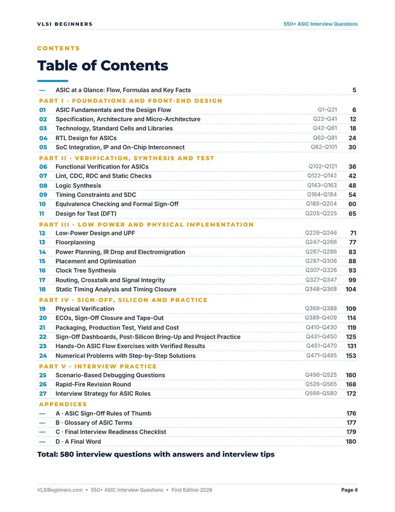
Table of contents listing 27 chapters in five parts with question ranges, plus four appendices
PAGE 4Contents and question ranges
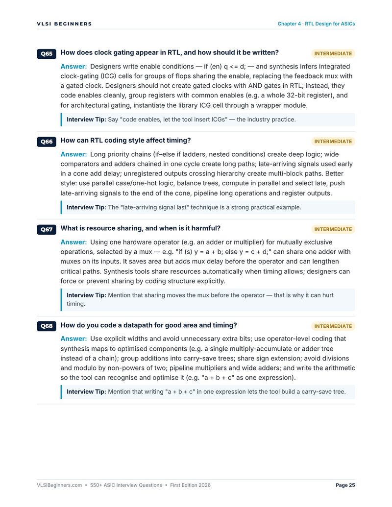
Chapter 4 page on clock gating in RTL, how coding style affects timing, resource sharing and datapath coding
CHAPTER 4RTL for timing and area
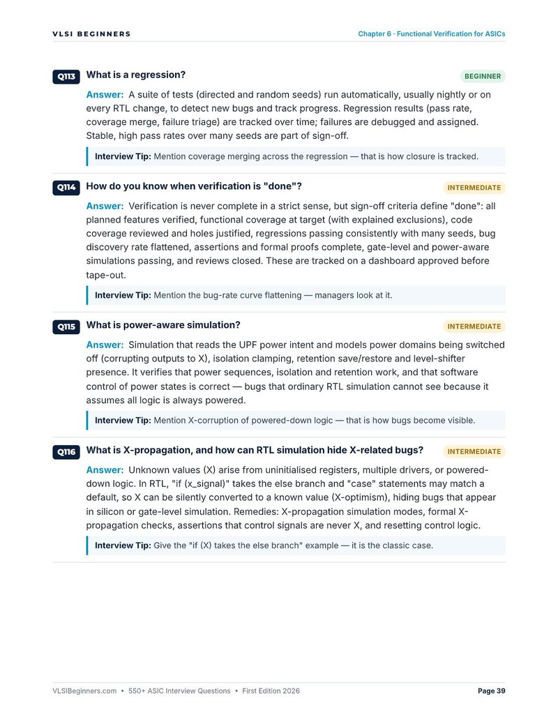
Chapter 6 page on regressions, deciding when verification is done, power-aware simulation and X-propagation
CHAPTER 6Verification sign-off
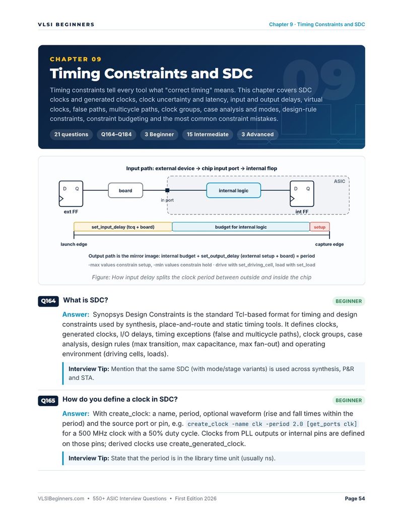
Chapter 9 opener with a diagram of how input delay splits the clock period, and questions on SDC and defining clocks
CHAPTER 9SDC and I/O budgets
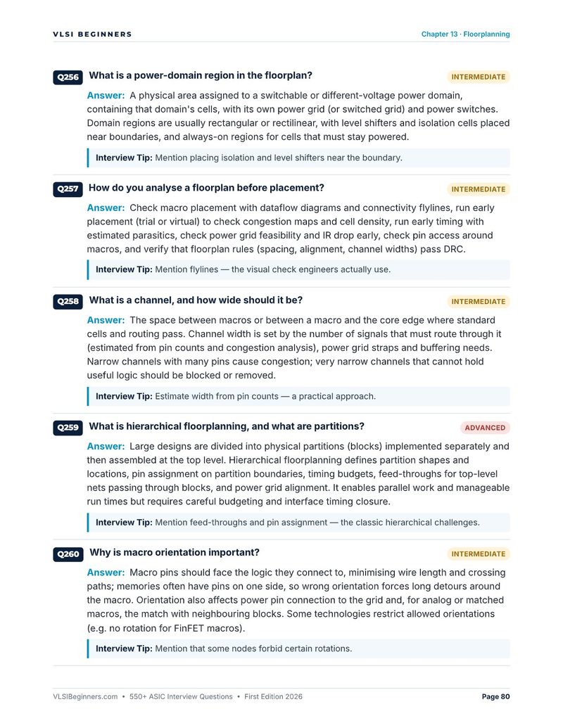
Chapter 13 page on power-domain regions, floorplan analysis, channels, hierarchical floorplanning and macro orientation
CHAPTER 13Floorplan decisions
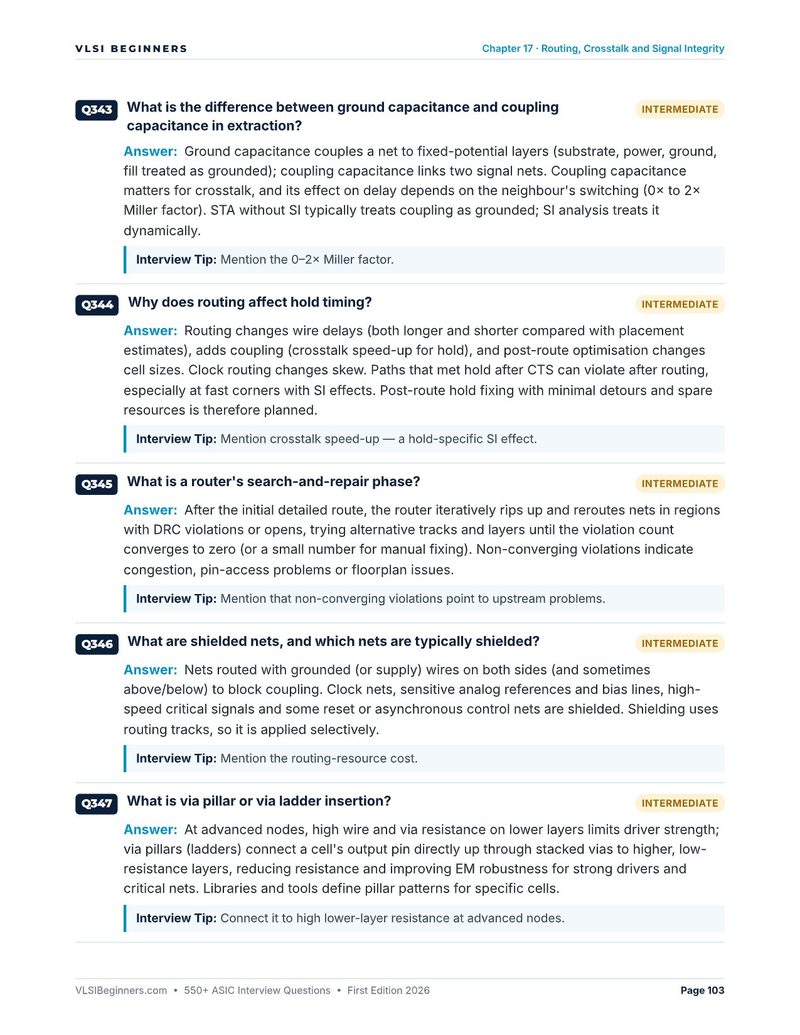
Chapter 17 page on ground and coupling capacitance, routing and hold, search-and-repair, shielding and via pillars
CHAPTER 17Routing and SI
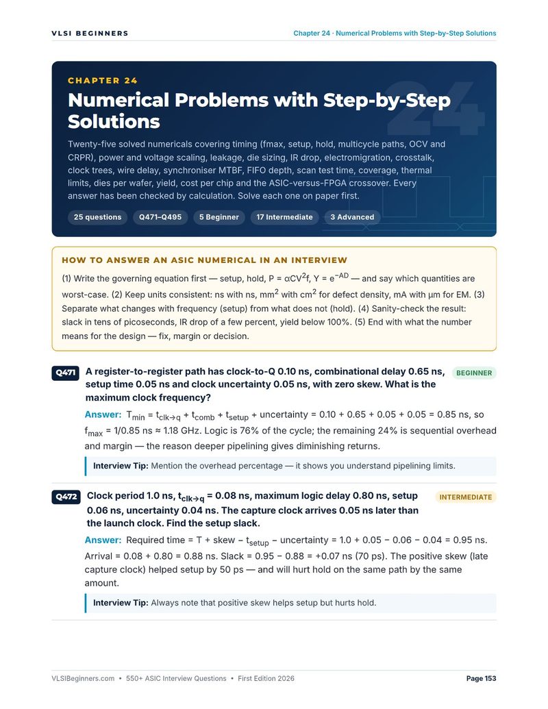
Chapter 24 opener with a method for answering ASIC numericals and two solved timing problems on fmax and setup slack
CHAPTER 24Solved numericals
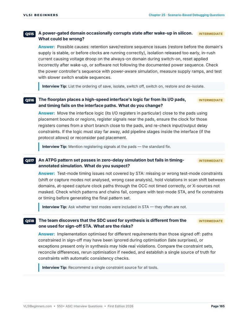
Chapter 25 page on state corruption after power-gating wake-up, interface logic far from its pads, ATPG patterns failing with timing, and mismatched synthesis and sign-off SDC
CHAPTER 25Debugging scenarios
HOW IT'S STRUCTURED

Five parts, in the order a chip is built

First the flow, architecture, libraries, RTL and SoC integration. Then verification, synthesis, constraints, equivalence and test, then low power and physical implementation through timing closure. After that come sign-off, tape-out and silicon, with exercises and numericals, and finally debugging under interview conditions.

PART I — FOUNDATIONS & FRONT-END DESIGN
From the idea to clean RTL
CH 1–5The ASIC flow, specification and micro-architecture, standard cells and libraries, RTL design for ASICs, SoC integration, IP and on-chip interconnect
101QUESTIONS
PART II — VERIFICATION, SYNTHESIS & TEST
Proving it, mapping it, constraining it
CH 6–11Functional verification, lint, CDC and RDC, logic synthesis, SDC timing constraints, equivalence checking and formal sign-off, design for test
124QUESTIONS
PART III — LOW POWER & PHYSICAL IMPLEMENTATION
From netlist to routed layout
CH 12–18Low-power design and UPF, floorplanning, power planning, IR drop and electromigration, placement, clock tree synthesis, routing and signal integrity, STA and timing closure
143QUESTIONS
PART IV — SIGN-OFF, SILICON & PRACTICE
From layout to working parts
CH 19–24Physical verification, ECOs and tape-out, packaging, production test, yield and cost, sign-off dashboards and bring-up, 20 hands-on exercises, 25 solved numericals
127QUESTIONS
PART V — INTERVIEW PRACTICE
Answering under pressure
CH 25–2730 scenario-based debugging questions, a 40-question rapid-fire round, and interview strategy for ASIC roles
85QUESTIONS
TOTAL ACROSS 27 CHAPTERS + 4 APPENDICES 580 questions
DIFFICULTY SPLIT
120 Beginner: the flow every candidate must know405 Intermediate: project-level practice and reports55 Advanced: silicon, sign-off and senior depth
SEE ALL 27 CHAPTERS
#CHAPTERQUESTIONS
PART I · FOUNDATIONS AND FRONT-END DESIGN
01ASIC Fundamentals and the Design FlowQ1–Q21
02Specification, Architecture and Micro-ArchitectureQ22–Q41
03Technology, Standard Cells and LibrariesQ42–Q61
04RTL Design for ASICsQ62–Q81
05SoC Integration, IP and On-Chip InterconnectQ82–Q101
PART II · VERIFICATION, SYNTHESIS AND TEST
06Functional Verification for ASICsQ102–Q121
07Lint, CDC, RDC and Static ChecksQ122–Q142
08Logic SynthesisQ143–Q163
09Timing Constraints and SDCQ164–Q184
10Equivalence Checking and Formal Sign-OffQ185–Q204
11Design for Test (DFT)Q205–Q225
PART III · LOW POWER AND PHYSICAL IMPLEMENTATION
12Low-Power Design and UPFQ226–Q246
13FloorplanningQ247–Q266
14Power Planning, IR Drop and ElectromigrationQ267–Q286
15Placement and OptimisationQ287–Q306
16Clock Tree SynthesisQ307–Q326
17Routing, Crosstalk and Signal IntegrityQ327–Q347
18Static Timing Analysis and Timing ClosureQ348–Q368
PART IV · SIGN-OFF, SILICON AND PRACTICE
19Physical VerificationQ369–Q388
20ECOs, Sign-Off Closure and Tape-OutQ389–Q409
21Packaging, Production Test, Yield and CostQ410–Q430
22Sign-Off Dashboards, Post-Silicon Bring-Up and Project PracticeQ431–Q450
23Hands-On ASIC Flow Exercises with Verified ResultsQ451–Q470
24Numerical Problems with Step-by-Step SolutionsQ471–Q495
PART V · INTERVIEW PRACTICE
25Scenario-Based Debugging QuestionsQ496–Q525
26Rapid-Fire Revision RoundQ526–Q565
27Interview Strategy for ASIC RolesQ566–Q580
APPENDICES
AASIC Sign-Off Rules of Thumbp. 176
BGlossary of ASIC Termsp. 177
CFinal Interview Readiness Checklistp. 179
DA Final Wordp. 180
FROM THE BOOK

Five questions, unedited

A two-minute timing numerical, an RTL habit for low power, the verification sign-off question managers ask, a senior floorplanning topic and a routing subtlety. All 580 follow the same format: the answer, then the tip that makes it stick.

Get the ebook now
Q471BEGINNER · NUMERICAL A register-to-register path has clock-to-Q 0.10 ns, combinational delay 0.65 ns, setup time 0.05 ns and clock uncertainty 0.05 ns, with zero skew. What is the maximum clock frequency? Tmin = tclk→q + tcomb + tsetup + uncertainty = 0.10 + 0.65 + 0.05 + 0.05 = 0.85 ns, so fmax = 1/0.85 ns ≈ 1.18 GHz. Logic is 76% of the cycle; the remaining 24% is sequential overhead and margin — the reason deeper pipelining gives diminishing returns. Tip: Mention the overhead percentage — it shows you understand pipelining limits.
Q65INTERMEDIATE · RTL FOR ASIC How does clock gating appear in RTL, and how should it be written? Designers write enable conditions — if (en) q <= d; — and synthesis infers integrated clock-gating (ICG) cells for groups of flops sharing the enable, replacing the feedback mux with a gated clock. Designers should not create gated clocks with AND gates in RTL; instead, they code enables cleanly, group registers with common enables (e.g. a whole 32-bit register), and for architectural gating, instantiate the library ICG cell through a wrapper module. Tip: Say “code enables, let the tool insert ICGs” — the industry practice.
Q114INTERMEDIATE · VERIFICATION How do you know when verification is “done”? Verification is never complete in a strict sense, but sign-off criteria define “done”: all planned features verified, functional coverage at target (with explained exclusions), code coverage reviewed and holes justified, regressions passing consistently with many seeds, bug discovery rate flattened, assertions and formal proofs complete, gate-level and power-aware simulations passing, and reviews closed. These are tracked on a dashboard approved before tape-out. Tip: Mention the bug-rate curve flattening — managers look at it.
Q259ADVANCED · FLOORPLANNING What is hierarchical floorplanning, and what are partitions? Large designs are divided into physical partitions (blocks) implemented separately and then assembled at the top level. Hierarchical floorplanning defines partition shapes and locations, pin assignment on partition boundaries, timing budgets, feed-throughs for top-level nets passing through blocks, and power grid alignment. It enables parallel work and manageable run times but requires careful budgeting and interface timing closure. Tip: Mention feed-throughs and pin assignment — the classic hierarchical challenges.
Q344INTERMEDIATE · ROUTING Why does routing affect hold timing? Routing changes wire delays (both longer and shorter compared with placement estimates), adds coupling (crosstalk speed-up for hold), and post-route optimisation changes cell sizes. Clock routing changes skew. Paths that met hold after CTS can violate after routing, especially at fast corners with SI effects. Post-route hold fixing with minimal detours and spare resources is therefore planned. Tip: Mention crosstalk speed-up — a hold-specific SI effect.
SEVEN DAYS LEFT?

The revision plan from the book

Answer aloud before reading. Redo every Chapter 24 numerical by hand, rebuild the Chapter 23 scripts and change one parameter at a time, and practise the Chapter 22 dashboard walk-through.

DAY 1Ch 1–5Flow, architecture, libraries, RTL for ASIC, SoC integration
DAY 2Ch 6–8Verification, lint, CDC and RDC, logic synthesis
DAY 3Ch 9–11SDC constraints, equivalence checking, DFT
DAY 4Ch 12–15Low power and UPF, floorplan, power planning, placement
DAY 5Ch 16–18CTS, routing and SI, STA and timing closure
DAY 6Ch 19–24PV, ECO and tape-out, yield, silicon, then exercises and numericals
DAY 7Ch 25–27Scenarios, rapid-fire round and the rules of thumb
WHO THIS IS FOR

For anyone who'll be asked to walk through the flow

ECE students and freshers

Campus drives and first ASIC or SoC interviews. Parts I and II turn a list of flow stages into answers that explain what each stage needs and produces.

RTL and verification engineers

Coding for timing, area and power, lint and CDC, synthesis results, SDC, equivalence and the downstream effects of front-end decisions.

Physical design and STA engineers

Floorplan, power grid, placement, CTS, routing, SI, timing closure, ECOs and sign-off, plus enough front-end and DFT to talk to every team.

DFT and product engineers

Scan, ATPG, BIST, test time, coverage, production test, yield and cost, and the silicon bring-up and failure-analysis scenarios.

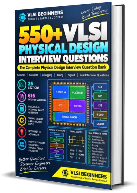
Physical Design Interview Questions ebook cover
GO DEEPER ON ONE STAGE

616 Physical Design Interview Questions

This book covers the whole flow. The Physical Design ebook goes deep on its back half: floorplanning, CTS, routing, timing closure, IR drop, EM, DRC/LVS, ECO and signoff, every question answered. The STA and DFT ebooks do the same for timing and test.

See the PD ebook

550+ ASIC Interview Questions

580 answered questions in 27 chapters, with solved numericals, hands-on exercises and debugging scenarios. Download the PDF straight after checkout.

Get the ebook now
QUESTIONS ABOUT THE BOOK
Are all 580 questions answered?

Yes. Every question has a full answer written the way you would explain it in an interview, plus an interview tip. The 25 numericals are solved step by step and checked by calculation, and the 20 hands-on exercises come with their verified results.

What format is it, and how fast do I get it?

A 181-page PDF. Checkout is on Topmate and the download is available right after payment.

Which roles is this book for?

RTL design, design verification, synthesis, physical design, STA and DFT roles, plus freshers and ECE students preparing for ASIC or SoC interviews. It covers the whole flow, so it also suits engineers moving from one stage of it to another.

Do I need commercial EDA tools?

No. The concept questions and numericals need only reasoning and a calculator. The 20 exercises were run with open-source tools (Yosys, Icarus Verilog and Python), so you can repeat them on a laptop.

How is this different from the Physical Design, STA and DFT ebooks?

This book covers the full flow end to end, from specification and RTL to tape-out and silicon bring-up, at the depth an ASIC interview expects. The Physical Design, STA and DFT ebooks each go much deeper into one stage.

Can I preview it?

Yes. Eight real pages are on this page, and the free ASIC Interview Questions page has 90+ sample questions with worked answers, solved numericals, the flow traced stage by stage and a timing slack calculator.

What's your refund policy?

Because this is a digital product delivered instantly, sales are generally final. If you hit a technical issue with your download, contact us within 7 days. See our Refund Policy for details.

Preparing for another round too? Browse all ebooks →