CMOS VLSI DESIGN INTERVIEW PREP

CMOS from the transistor up. 580 questions, each one answered.

MOSFET physics to SRAM, power and reliability in 27 chapters. Each answer is phrased for saying out loud, with a tip on the follow-up the interviewer is likely to ask. Includes 20 SPICE and switch-level exercises, 25 solved numericals and 30 silicon debugging scenarios.

181-PAGE PDF · INSTANT DOWNLOAD · 8 FREE PREVIEW PAGES BELOW
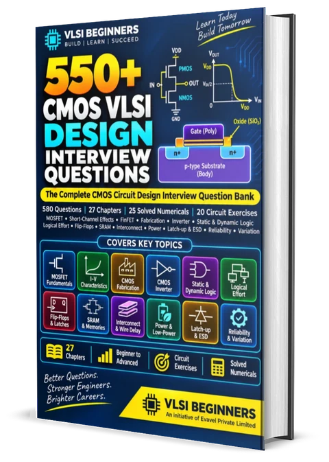
550+ CMOS VLSI Design Interview Questions ebook cover — VLSI Beginners
580
QUESTIONS WITH ANSWERS
27
CHAPTERS IN 5 PARTS
25
SOLVED NUMERICALS
20
SPICE & CIRCUIT EXERCISES
THE PROBLEM

"Draw a NAND gate" is never the whole question

CMOS rounds test what sits under the logic you design, place and time. They show up in circuit, memory and standard-cell interviews, and in physical design, STA and analog-layout rounds too.

The definition is only the opening line. Next comes: which input goes nearest the output, why the inverter's switching point barely moves when you resize it, what the keeper fights against, how a 6T cell reads without flipping, why the slow corner can be the cold one, and what causes latch-up.

The book follows the same path as a chip: the transistor and how it's made, then the inverter and every logic style, then storage, memory, wires and power, then layout, reliability and variation, and finally the interview itself.

WHAT'S INSIDE

From device equations to silicon failures

A CMOS round asks you to explain the physics, size a circuit, estimate a number and diagnose a chip. The book prepares each of those separately.

ANSWERS

An answer and a tip for all 580

Every question carries a Beginner, Intermediate or Advanced tag, a concise spoken-style answer, and an Interview Tip naming the follow-up or the detail most candidates leave out.

CIRCUITS

20 SPICE and switch-level exercises

Inverter VTC and delay, NAND, NOR and AOI21 sizing, a transmission-gate mux, a ring oscillator, a domino gate with keeper, a TG latch, a 6T SRAM cell, a level shifter, the stack effect, an RC wire and an SRAM butterfly curve.

NUMERICALS

25 calculations, every step shown

Drain current and body effect, subthreshold leakage, VM, RC delay, logical-effort paths, buffer chains, charge sharing, wire delay and repeaters, mismatch, SRAM and DRAM sensing, EM width, IR drop and DVFS.

DIAGRAMS

The curves interviewers ask you to draw

MOSFET output and subthreshold curves, the inverter transfer characteristic, transistor-level gates and cells, and a cell characterisation report across PVT corners, read line by line.

DEBUGGING

30 real silicon scenarios

SRAM bits flipping on read, writes failing at the SF corner, domino failing when the clock is slowed, leakage 3× over budget, slow-cold timing failures, wake-up droop from power gating and ageing after burn-in.

QUICK REVISION

For the night before

A formula sheet, a circuit-style selection guide, a 30-question rapid-fire round, a glossary of CMOS terms, a 7-day plan and a final readiness checklist.

LOOK INSIDE

Read eight real pages first

Straight from the PDF you'll download. Tap any page to open it full size.

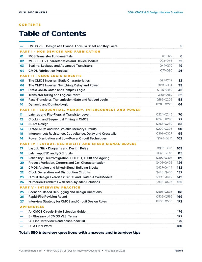
Table of contents listing 27 chapters in five parts with question ranges, plus four appendices
PAGE 4Contents and question ranges
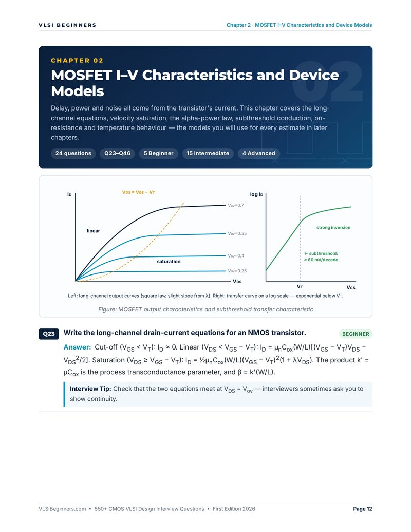
Chapter 2 opener with MOSFET output characteristics and a log-scale subthreshold transfer curve, and the long-channel drain-current equations
CHAPTER 2I–V and subthreshold curves
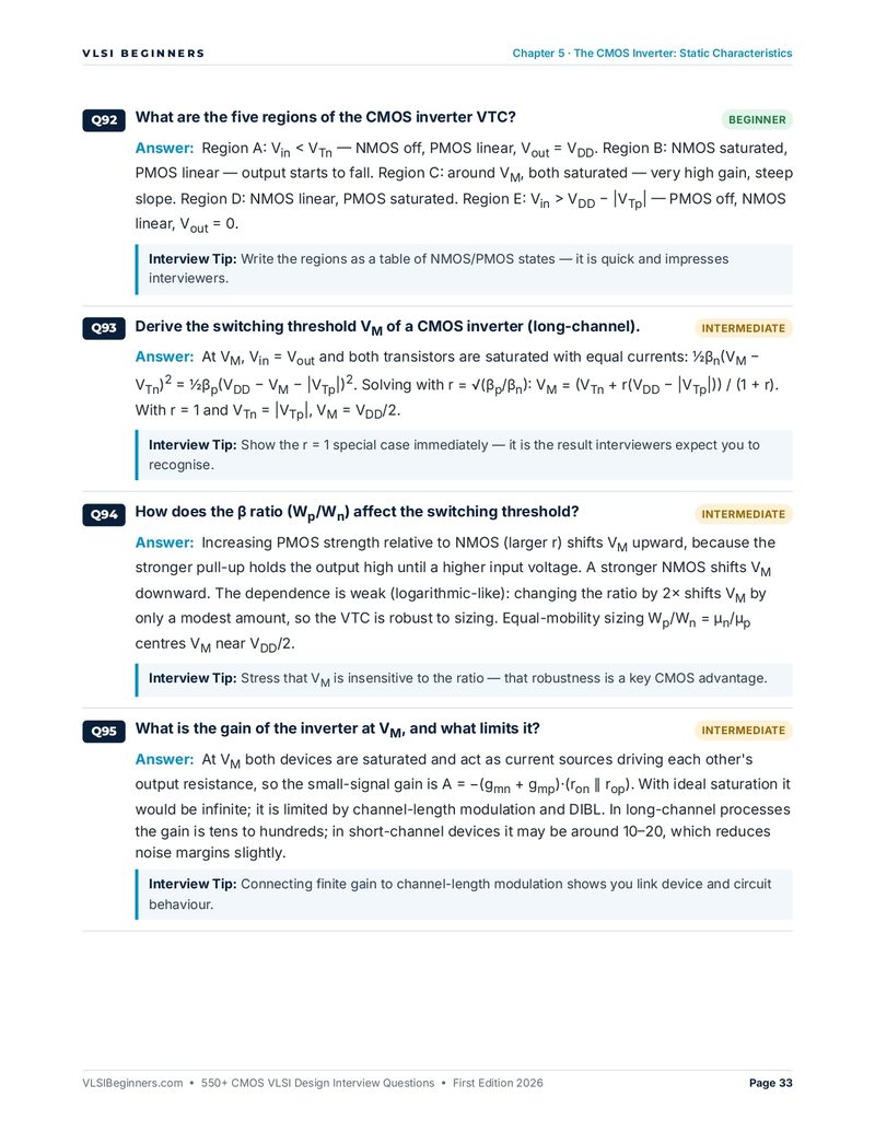
Chapter 5 page on the five regions of the inverter VTC, deriving the switching threshold, the beta ratio and mid-point gain
CHAPTER 5Inverter VTC and VM
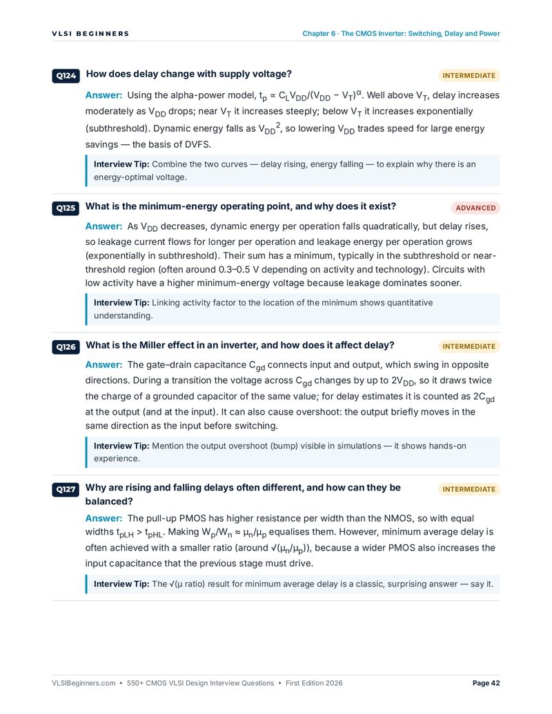
Chapter 6 page on delay versus supply voltage, the minimum-energy point, the Miller effect and balancing rise and fall delays
CHAPTER 6Delay, energy and Miller effect
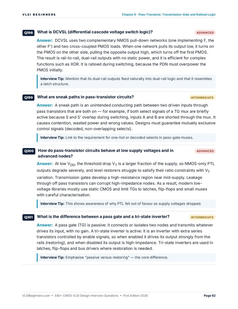
Chapter 9 page on DCVSL, sneak paths, pass-transistor logic at low voltage and pass gates versus tri-state inverters
CHAPTER 9DCVSL and pass-gate pitfalls
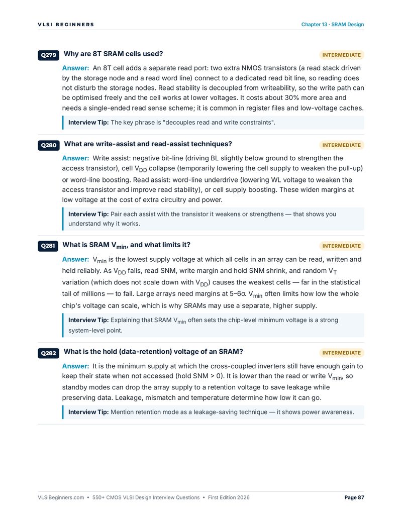
Chapter 13 page on 8T SRAM cells, read and write assist techniques, SRAM Vmin and data-retention voltage
CHAPTER 138T cells, assists and Vmin
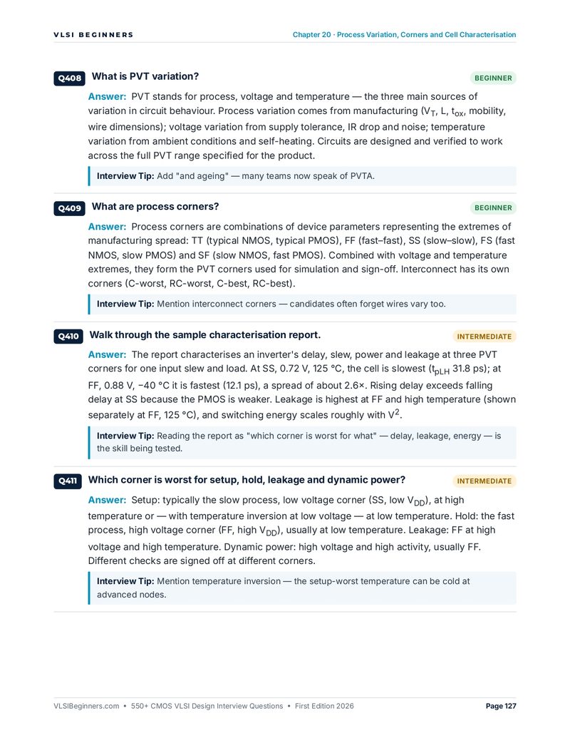
Chapter 20 page on PVT variation, process corners, reading a characterisation report and worst corners for setup, hold, leakage and power
CHAPTER 20PVT corners, explained
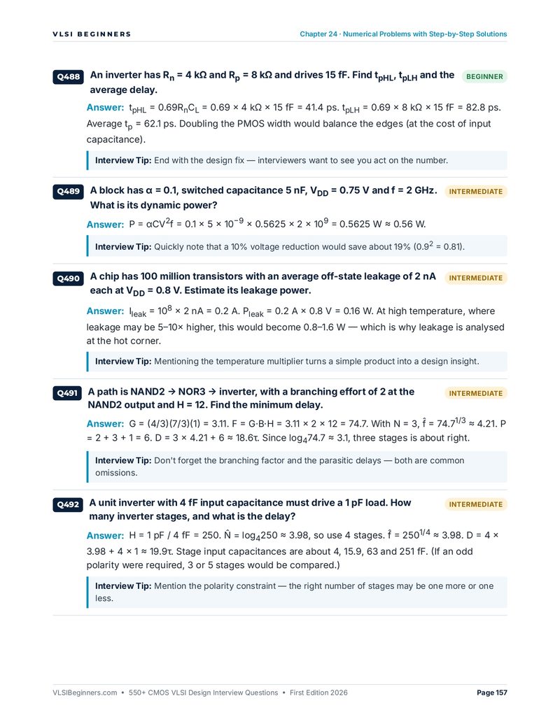
Chapter 24 page with solved problems on inverter RC delay, dynamic and leakage power, a logical-effort path and a buffer chain
CHAPTER 24Delay, power and logical effort, solved
HOW IT'S STRUCTURED

Five parts, from one transistor to a reliable chip

Start with the device and how it's built. Turn it into logic, then into storage, memory, wires and power. Then make it manufacturable and reliable, and finish by practising answers under interview conditions.

PART I — MOS DEVICES & FABRICATION
The physics every later answer leans on
CH 1–4MOS transistor fundamentals, I–V characteristics and models, scaling, leakage, FinFET and GAA, the CMOS fabrication process
90QUESTIONS
PART II — CMOS LOGIC CIRCUITS
The heart of a circuit round
CH 5–10Inverter static behaviour, inverter switching, delay and power, static CMOS gates, transistor sizing and logical effort, pass-transistor, transmission-gate and ratioed logic, dynamic and domino logic
133QUESTIONS
PART III — SEQUENTIAL, MEMORY, INTERCONNECT & POWER
Where speed, area and power collide
CH 11–16Transistor-level latches and flip-flops, clocking and sequential timing, SRAM design, DRAM, ROM and non-volatile memory, interconnect delay and crosstalk, power and low-power techniques
128QUESTIONS
PART IV — LAYOUT, RELIABILITY & MIXED-SIGNAL
What separates juniors from seniors
CH 17–24Layout, stick diagrams and design rules, latch-up, ESD and I/O, electromigration, HCI, BTI and TDDB, variation and corners, analog building blocks, clock circuits, 20 circuit exercises, 25 solved numericals
154QUESTIONS
PART V — INTERVIEW PRACTICE
Answering under pressure
CH 25–2730 scenario-based debugging and design questions, a 30-question rapid-fire round, and interview strategy for CMOS and circuit design roles
75QUESTIONS
TOTAL ACROSS 27 CHAPTERS + 4 APPENDICES 580 questions
DIFFICULTY SPLIT
122 Beginner: core concepts401 Intermediate: sizing, analysis and trade-offs57 Advanced: silicon and sign-off depth
SEE ALL 27 CHAPTERS
#CHAPTERQUESTIONS
PART I · MOS DEVICES AND FABRICATION
01MOS Transistor FundamentalsQ1–Q22
02MOSFET I–V Characteristics and Device ModelsQ23–Q46
03Scaling, Leakage and Advanced TransistorsQ47–Q70
04CMOS Fabrication ProcessQ71–Q90
PART II · CMOS LOGIC CIRCUITS
05The CMOS Inverter: Static CharacteristicsQ91–Q112
06The CMOS Inverter: Switching, Delay and PowerQ113–Q134
07Static CMOS Gates and Complex LogicQ135–Q160
08Transistor Sizing and Logical EffortQ161–Q182
09Pass-Transistor, Transmission-Gate and Ratioed LogicQ183–Q202
10Dynamic and Domino LogicQ203–Q223
PART III · SEQUENTIAL, MEMORY, INTERCONNECT AND POWER
11Latches and Flip-Flops at Transistor LevelQ224–Q245
12Clocking and Sequential Timing in CMOSQ246–Q265
13SRAM DesignQ266–Q289
14DRAM, ROM and Non-Volatile Memory CircuitsQ290–Q305
15Interconnect: Resistance, Capacitance, Delay and CrosstalkQ306–Q327
16Power Dissipation and Low-Power Circuit TechniquesQ328–Q351
PART IV · LAYOUT, RELIABILITY AND MIXED-SIGNAL BLOCKS
17Layout, Stick Diagrams and Design RulesQ352–Q371
18Latch-up, ESD and I/O CircuitsQ372–Q391
19Reliability: Electromigration, HCI, BTI, TDDB and AgeingQ392–Q407
20Process Variation, Corners and Cell CharacterisationQ408–Q426
21CMOS Analog and Mixed-Signal Building BlocksQ427–Q444
22Clock Generation and Distribution CircuitsQ445–Q460
23Circuit Design Exercises: SPICE and Switch-Level ModelsQ461–Q480
24Numerical Problems with Step-by-Step SolutionsQ481–Q505
PART V · INTERVIEW PRACTICE
25Scenario-Based Debugging and Design QuestionsQ506–Q535
26Rapid-Fire Revision RoundQ536–Q565
27Interview Strategy for CMOS and Circuit Design RolesQ566–Q580
APPENDICES
ACMOS Circuit-Style Selection Guidep. 176
BGlossary of CMOS VLSI Termsp. 177
CFinal Interview Readiness Checklistp. 179
DA Final Wordp. 180
FROM THE BOOK

Five questions, word for word

A speed metric, a sizing trick, a leakage effect, a dynamic-logic trade-off and a sign-off surprise. Each of the 580 follows the same shape: the answer, then the tip that sets you apart.

Get the ebook now
Q117BEGINNER What is FO4 delay? FO4 delay is the delay of an inverter driving four identical copies of itself. It is a technology-normalised speed metric: circuit delays are often quoted in FO4 units (for example, a processor cycle of 20 FO4) so that designs can be compared across nodes. Roughly, FO4 ≈ 5× the intrinsic delay τ of a unit inverter driving itself. Tip: Quoting cycle times in FO4 shows you think in technology-independent terms.
Q148INTERMEDIATE · SIZING Where should the latest-arriving input be placed in a series stack, and why? On the transistor closest to the output. When the earlier inputs arrive, the transistors nearer the rail turn on first and discharge the internal nodes in advance; when the critical input finally switches, only the output capacitance and the top transistor's path remain. Placing it nearest the rail leaves all internal capacitances to discharge after it arrives. Tip: This input-ordering trick is a classic. Explain the internal-node discharge reasoning.
Q69INTERMEDIATE · LEAKAGE What is the "stack effect"? When two or more off transistors are in series, the intermediate node rises to a small positive voltage. This makes VGS of the upper transistor negative, raises its VT through body effect and reduces VDS of each device (reducing DIBL), so the stack leaks much less than a single off transistor, often by 5–10×. Tip: Explain all three mechanisms. Most candidates mention only one.
Q211INTERMEDIATE · DYNAMIC LOGIC What is a keeper transistor, and how is it sized? A weak PMOS from VDD to the dynamic node, its gate driven by the domino inverter output. While the node is high it stays on, replacing charge lost to leakage, charge sharing and noise. It must be weak enough that the evaluation network can still discharge the node against it, so it is typically about 10% of the pull-down strength. Tip: Frame keeper sizing as a noise-versus-speed trade-off.
Q514INTERMEDIATE · SCENARIO A design meets timing at the slow-hot corner but fails at the slow-cold corner in silicon at low voltage. Explain. Temperature inversion: at low supply voltage in advanced nodes, the threshold-voltage increase at low temperature outweighs the mobility gain, so gates are slower when cold. If sign-off only analysed the hot corner, cold-corner setup failures were missed. Add slow-cold corners at low voltage to sign-off, or raise the supply when cold. Tip: Naming temperature inversion and its consequence for sign-off is the expected answer.
INTERVIEW NEXT WEEK?

The 7-day plan printed in the book

Say each answer before you read it. Sketch the I–V curves, the inverter VTC, NAND, NOR and AOI networks and the 6T cell from memory, and solve every problem in Chapters 8 and 24 on paper.

DAY 1Ch 1–3MOSFET physics, I–V models, short-channel effects, FinFET and GAA
DAY 2Ch 4–6Fabrication, inverter VTC, delay, power, FO4 and buffer sizing
DAY 3Ch 7–10Static gates, logical effort, pass-transistor and dynamic logic
DAY 4Ch 11–14Flip-flops, clocking, SRAM, DRAM and non-volatile memory
DAY 5Ch 15–17Interconnect, low-power techniques, layout and design rules
DAY 6Ch 18–22ESD and latch-up, reliability, variation, analog and clock circuits
DAY 7Ch 23–27SPICE exercises, numericals, scenarios, rapid-fire and formula sheet
WHO THIS IS FOR

Anyone whose interview goes below the gate level

ECE students and freshers

CMOS is in almost every core-company written test and first round. Parts I and II turn lecture notes into answers you can say in a minute.

Circuit, memory and standard-cell roles

Sizing, logical effort, dynamic logic, flip-flop design, SRAM margins and assists, level shifters, characterisation and corners.

Physical design and STA engineers

Wire RC and repeaters, crosstalk, IR drop, electromigration, latch-up rules, temperature inversion and why cells behave as they do.

Self-learners

Every answer, deck and calculation is in the book, so you can check your own reasoning without a mentor.

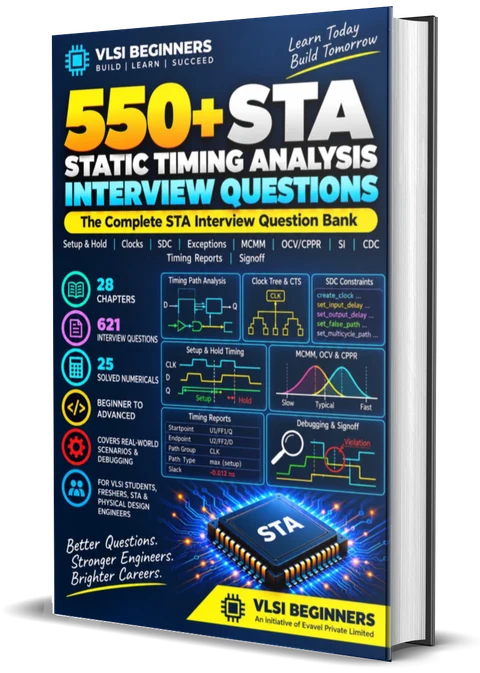
550+ STA Interview Questions ebook cover
PAIRS WELL WITH

550+ STA Interview Questions

This book explains why a cell has the delay, slew and leakage it does. The STA ebook takes those numbers into timing sign-off: 621 answered questions on setup and hold, SDC, OCV, corners and reading timing reports.

See the STA ebook

550+ CMOS VLSI Design Interview Questions

580 answered questions in 27 chapters, with circuit exercises, numericals and silicon debugging. The PDF is yours as soon as you check out.

Get the ebook now
QUESTIONS ABOUT THE BOOK
Does every question have an answer?

Yes. All 580 questions have a full answer written the way you would say it in an interview, plus an interview tip. The 20 circuit exercises include complete SPICE decks or switch-level Verilog, and the 25 numericals are solved step by step.

What do I get after paying?

A 181-page PDF. You check out on Topmate and can download it straight away.

I'm applying for physical design or STA, not circuit design. Is it still useful?

Yes. PD and STA rounds lean on CMOS for delay, slew, leakage, wire RC, crosstalk, IR drop, electromigration, corners and cell characterisation. Those topics have their own chapters, along with layout, latch-up and design rules.

Is it too advanced for a fresher?

No. 122 questions are marked Beginner, Chapter 1 starts from what a MOSFET is, and the rapid-fire round is mostly beginner level. Advanced questions are tagged, so you can leave them for later.

Do I need a SPICE simulator or a foundry PDK?

No. The exercises use plain SPICE syntax with simple built-in models, so you can read them as worked answers or run them in a free simulator. Numbers in the book are representative values chosen to teach the method.

Can I read some of it first?

Yes. Eight real pages are on this page, and the free CMOS Interview Questions page has 90+ sample questions with worked answers, solved numericals and an inverter delay and power calculator.

What's your refund policy?

Because this is a digital product delivered instantly, sales are generally final. If you hit a technical issue with your download, contact us within 7 days. See our Refund Policy for details.

Preparing for another round too? Browse all ebooks →