FPGA DESIGN INTERVIEW PREP

570 FPGA questions. Every one answered.

From LUTs and RTL to timing closure, CDC, transceivers and lab debug, in 25 chapters. Every answer is written the way you'd say it in an interview, with a tip for the follow-up. Includes 25 coding exercises with solutions, 25 solved numericals and 30 debugging scenarios.

146-PAGE PDF · INSTANT DOWNLOAD · 10 FREE PREVIEW PAGES BELOW
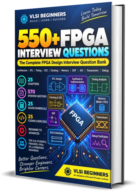
550+ FPGA Interview Questions ebook cover — VLSI Beginners
570
QUESTIONS, ALL ANSWERED
25
CODING EXERCISES
25
SOLVED NUMERICALS
30
DEBUG SCENARIOS
THE PROBLEM

FPGA interviews test what you can build and debug

FPGA engineering is one of the most hands-on VLSI careers, and the interviews reflect it. You'll be asked to write RTL on a whiteboard, explain why a design fails timing, choose a CDC technique, size a FIFO, read a timing report, or say why a board works in simulation but not in the lab.

Most FPGA prep material is either too basic or too vendor-specific. It explains what a LUT is, then skips the questions that decide offers: clock planning, async FIFOs, BRAM sizing, fixed-point bit growth, AXI handshakes, transceiver bring-up and on-chip debug.

This book follows the order a real FPGA project runs: architecture, RTL and timing first, then clocks, CDC, memory, DSP and interfaces, then verification, debug and production, and finally the interview itself.

WHAT'S INSIDE

More than a question list

FPGA interviews test four skills: explaining a concept, writing RTL, working out a number and debugging hardware. The book trains each one.

CONCEPTS

An answer and a tip for every question

Each of the 570 questions has a difficulty level, an interview-ready answer, and an Interview Tip: the follow-up question or common mistake the interviewer is listening for.

CODING

25 HDL exercises with solutions

Synchronisers, clock enables instead of divided clocks, debouncers, PWM, Gray converters, sequence-detector FSMs, SRL shift registers, FIFOs and moving-average filters, in clean always_ff style.

NUMERICALS

25 solved problems, step by step

fmax and setup slack, pipelining, MMCM/PLL dividers, related-clock edges, BRAM and LUT-RAM sizing, FIFO depth, MTBF, Q-format and bit growth, NCO tuning words, AXI, DDR and PCIe bandwidth.

TIMING

Constraints and closure, properly

XDC/SDC clocks, generated clocks, I/O delays, clock groups and exceptions, reading report_timing_summary, and the closure toolbox from pipelining to physical optimisation.

SYSTEMS

The blocks real designs are built from

Clocking and CDC, BRAM, UltraRAM and FIFOs, DSP slices and fixed point, I/O standards, high-speed transceivers, AXI and AXI-Stream, SoC FPGAs, HLS and partial reconfiguration.

REVISION KIT

Built for the night before

A formula sheet with a memory-resource table, a 30-question rapid-fire round, a constraints and primitives quick reference, a glossary, a 7-day plan and a readiness checklist.

LOOK INSIDE

Read ten real pages before you buy

These are pages from the actual PDF, not mockups. Click any page to zoom in and read it in full.

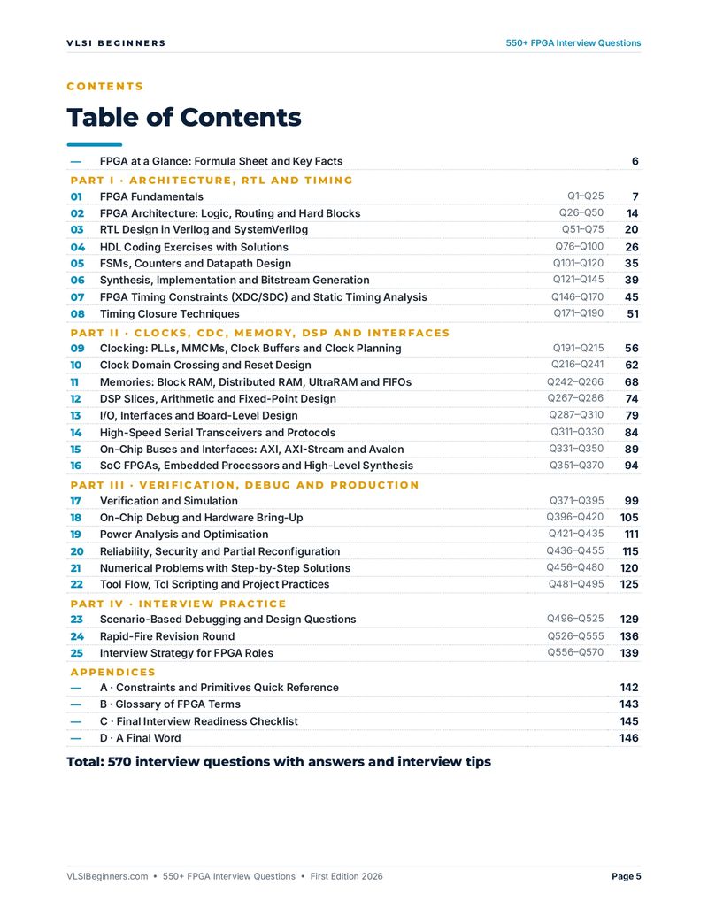
Table of contents showing 25 chapters in four parts and four appendices, totalling 570 questions
PAGE 5Contents: all 25 chapters
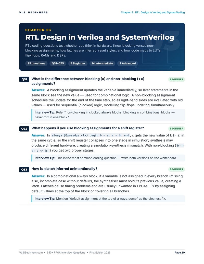
Chapter 3 opener on blocking and non-blocking assignments, shift registers and unintended latch inference
CHAPTER 3Blocking vs non-blocking, latches
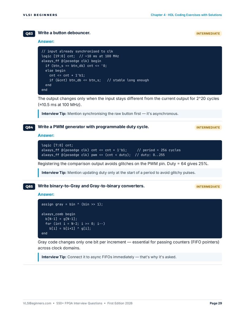
Chapter 4 page with SystemVerilog solutions for a button debouncer, a PWM generator and binary-to-Gray converters
CHAPTER 4Coding exercises with solutions
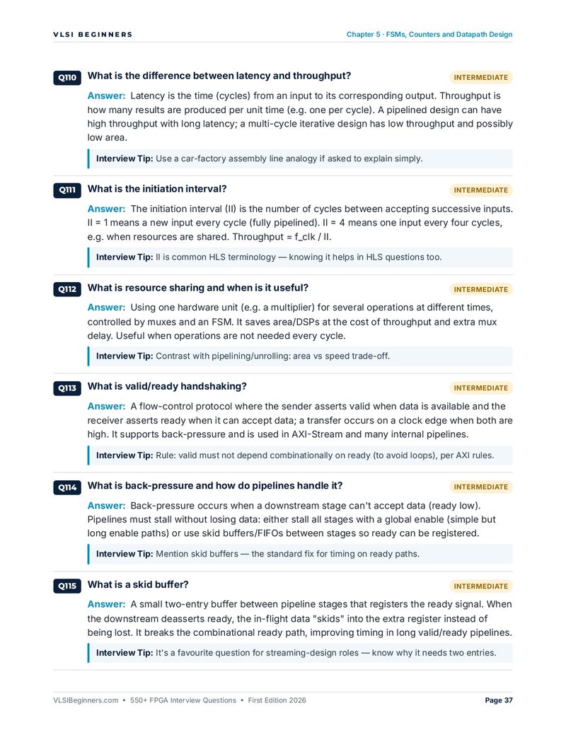
Chapter 5 page on latency vs throughput, initiation interval, resource sharing, valid/ready handshaking, back-pressure and skid buffers
CHAPTER 5Latency, valid/ready, skid buffers
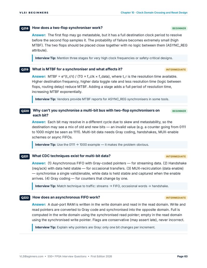
Chapter 10 page on two-flop synchronisers, MTBF, multi-bit CDC techniques and asynchronous FIFOs
CHAPTER 10Synchronisers and async FIFOs
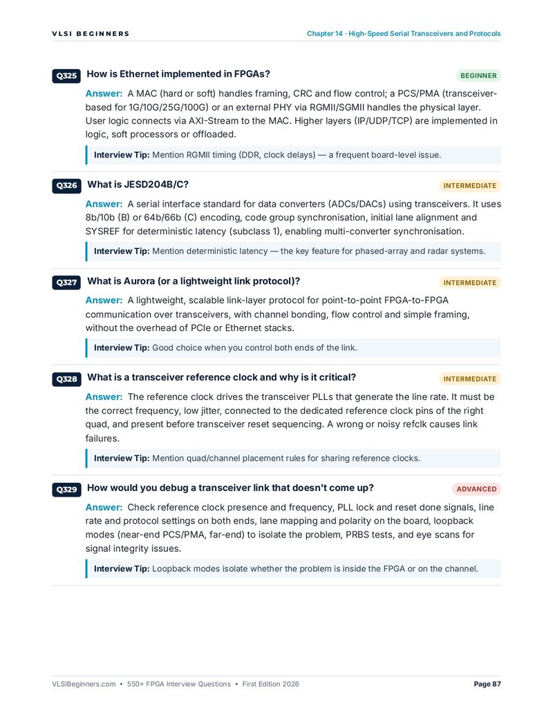
Chapter 14 page on Ethernet in FPGAs, JESD204B/C, Aurora, reference clocks and debugging a transceiver link
CHAPTER 14Ethernet, JESD204, link debug
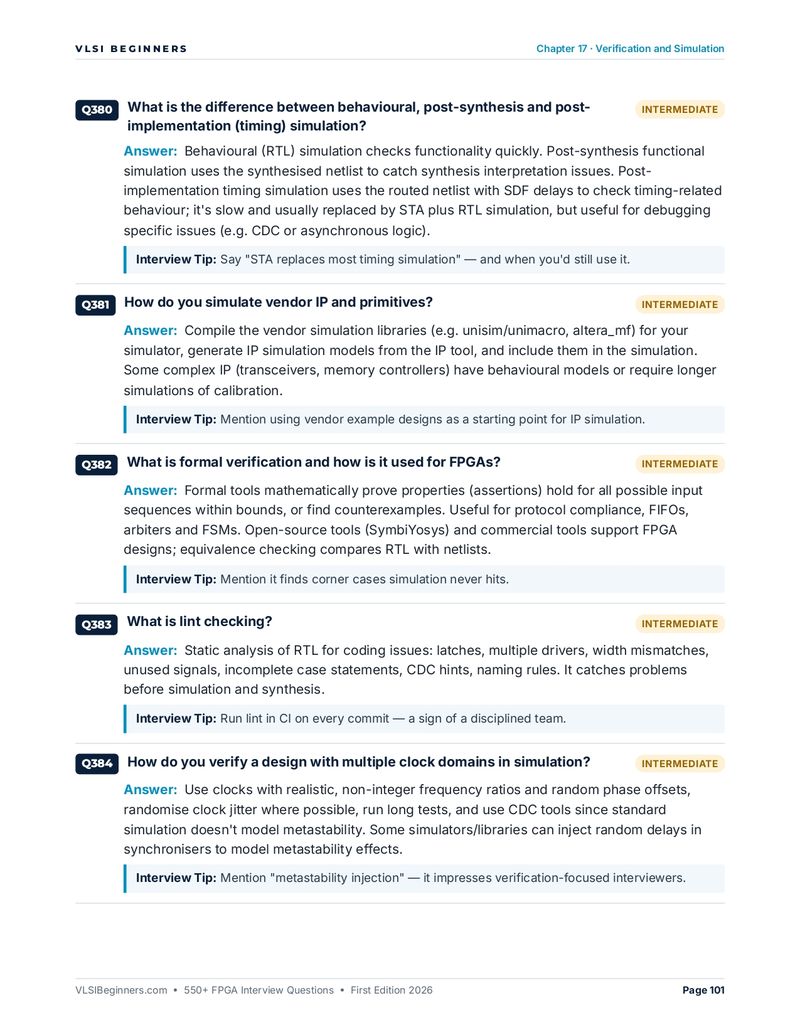
Chapter 17 page on behavioural vs timing simulation, vendor IP simulation, formal verification, lint and multi-clock verification
CHAPTER 17Simulation, formal, lint
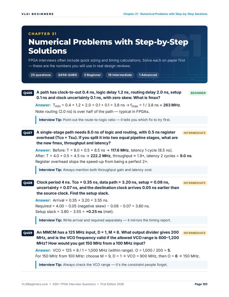
Chapter 21 opener with solved numericals on fmax, pipelining, setup slack and MMCM divider settings
CHAPTER 21Solved numericals
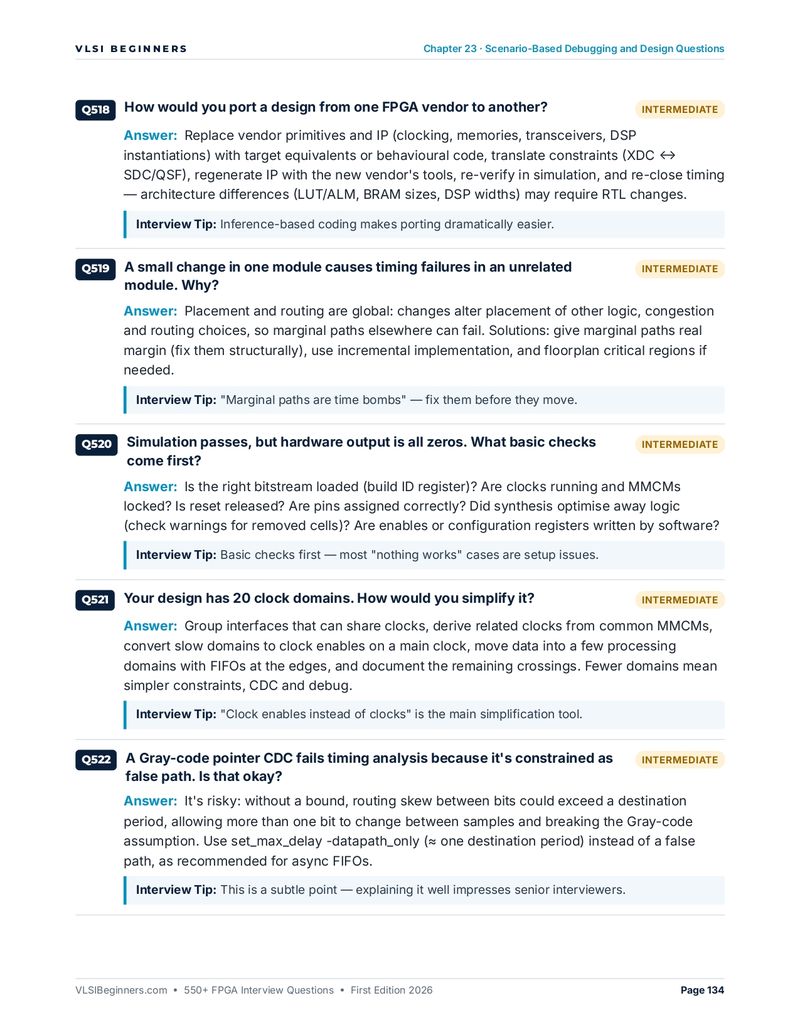
Chapter 23 page on vendor porting, timing changes in unrelated modules, hardware outputting zeros, clock-domain reduction and Gray-pointer constraints
CHAPTER 23Debugging and design scenarios
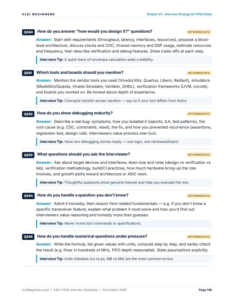
Chapter 25 page on answering design questions, which tools to mention, debugging maturity and handling numericals under pressure
CHAPTER 25Interview strategy
HOW IT'S STRUCTURED

Four parts, from LUTs to lab bring-up

The chapters follow the order of a real FPGA project: architecture, RTL and timing first, then clocks, memory, DSP and interfaces, then verification, debug and production, and finally the interview itself.

PART I — ARCHITECTURE, RTL & TIMING
What every FPGA interview checks
CH 1–8FPGA fundamentals, logic, routing and hard blocks, RTL in Verilog and SystemVerilog, 25 coding exercises, FSMs and datapaths, synthesis and bitstreams, XDC/SDC and STA, timing closure
190QUESTIONS
PART II — CLOCKS, CDC, MEMORY, DSP & INTERFACES
The building blocks of real designs
CH 9–16PLLs, MMCMs and clock planning, CDC and resets, BRAM, distributed RAM, UltraRAM and FIFOs, DSP and fixed point, I/O and board design, transceivers, AXI and Avalon, SoC FPGAs and HLS
180QUESTIONS
PART III — VERIFICATION, DEBUG & PRODUCTION
What separates juniors from seniors
CH 17–22Verification and simulation, on-chip debug and hardware bring-up, power, reliability, security and partial reconfiguration, 25 solved numericals, tool flow and Tcl scripting
125QUESTIONS
PART IV — INTERVIEW PRACTICE
Rehearsing the real thing
CH 23–2530 scenario-based debugging and design questions, a 30-question rapid-fire round, and interview strategy for FPGA roles
75QUESTIONS
TOTAL ACROSS 25 CHAPTERS + 4 APPENDICES 570 questions
DIFFICULTY SPLIT
142 Beginner: fundamentals every candidate must know384 Intermediate: expected with project exposure44 Advanced: architecture and senior-level depth
SEE ALL 25 CHAPTERS
#CHAPTERQUESTIONS
PART I · ARCHITECTURE, RTL AND TIMING
01FPGA FundamentalsQ1–Q25
02FPGA Architecture: Logic, Routing and Hard BlocksQ26–Q50
03RTL Design in Verilog and SystemVerilogQ51–Q75
04HDL Coding Exercises with SolutionsQ76–Q100
05FSMs, Counters and Datapath DesignQ101–Q120
06Synthesis, Implementation and Bitstream GenerationQ121–Q145
07FPGA Timing Constraints (XDC/SDC) and Static Timing AnalysisQ146–Q170
08Timing Closure TechniquesQ171–Q190
PART II · CLOCKS, CDC, MEMORY, DSP AND INTERFACES
09Clocking: PLLs, MMCMs, Clock Buffers and Clock PlanningQ191–Q215
10Clock Domain Crossing and Reset DesignQ216–Q241
11Memories: Block RAM, Distributed RAM, UltraRAM and FIFOsQ242–Q266
12DSP Slices, Arithmetic and Fixed-Point DesignQ267–Q286
13I/O, Interfaces and Board-Level DesignQ287–Q310
14High-Speed Serial Transceivers and ProtocolsQ311–Q330
15On-Chip Buses and Interfaces: AXI, AXI-Stream and AvalonQ331–Q350
16SoC FPGAs, Embedded Processors and High-Level SynthesisQ351–Q370
PART III · VERIFICATION, DEBUG AND PRODUCTION
17Verification and SimulationQ371–Q395
18On-Chip Debug and Hardware Bring-UpQ396–Q420
19Power Analysis and OptimisationQ421–Q435
20Reliability, Security and Partial ReconfigurationQ436–Q455
21Numerical Problems with Step-by-Step SolutionsQ456–Q480
22Tool Flow, Tcl Scripting and Project PracticesQ481–Q495
PART IV · INTERVIEW PRACTICE
23Scenario-Based Debugging and Design QuestionsQ496–Q525
24Rapid-Fire Revision RoundQ526–Q555
25Interview Strategy for FPGA RolesQ556–Q570
APPENDICES
AConstraints and Primitives Quick Referencep. 142
BGlossary of FPGA Termsp. 143
CFinal Interview Readiness Checklistp. 145
DA Final Wordp. 146
FROM THE BOOK

Five real questions, as printed

A coding exercise, a timing-closure question, a CDC question, a numerical and a lab-debug scenario. Every question in the book has the same parts: a direct answer and an interview tip.

Get the ebook now
Q79BEGINNER · CODING Write a clock divider by 2 without creating a new clock domain. Use a clock enable: always_ff @(posedge clk) tog <= ~tog; then if (tog) slow_q <= slow_d;. The logic still runs on the original clock, so there's one domain and no extra skew. If a real divided clock is needed, generate it with an MMCM/PLL or a clock-buffer divider. Tip: Interviewers want to hear "clock enable, not a logic-generated clock".
Q172BEGINNER · TIMING What is the first thing you check when timing fails? Whether the constraints are correct: clock periods, clock groups for asynchronous crossings, required multicycle or false paths, and realistic I/O delays. Many "violations" are constraint errors, such as timed paths between unrelated clocks. Tip: "Validate constraints before changing RTL" is the professional first step.
Q220BEGINNER · CDC Why can't you synchronise a multi-bit bus with two-flop synchronisers on each bit? Each bit may resolve in a different cycle, so the destination can see a mix of old and new bits: a counter going from 0111 to 1000 might be seen as 1111. Multi-bit data needs Gray coding, handshakes, mux-enable schemes or async FIFOs. Tip: Use the 0111 → 1000 example. It makes the problem obvious.
Q464INTERMEDIATE · NUMERICAL A producer writes a 512-word burst at 250 MHz; the consumer reads continuously at 200 MHz. Minimum FIFO depth? Burst lasts 512 / 250 MHz = 2.048 µs; words read meanwhile = 409.6. Depth ≥ 512 − 409.6 = 102.4 → 103 words, plus synchroniser and latency margin, so choose 128. Tip: Round up to a power of two and state your margin assumption.
Q500INTERMEDIATE · SCENARIO After adding an ILA, the bug disappears. What does it suggest? Timing or CDC sensitivity: the ILA changed placement. Check timing reports against all constraints, CDC reports, unconstrained paths and marginal paths near the bug. Use incremental compile for debug, or keep permanent debug infrastructure so placement doesn't shift. Tip: Heisenbugs almost always point to timing or CDC.
INTERVIEW IN A WEEK?

The 7-day revision plan from the book

Answer each question aloud before reading the answer. Write every coding exercise on paper without looking, and sketch the async FIFO, the synchroniser and the valid/ready handshake until you can draw them from memory.

DAY 1Ch 1–3Fundamentals, architecture, RTL coding rules
DAY 2Ch 4–5Write every coding exercise; FSMs and datapaths
DAY 3Ch 6–8Synthesis, constraints, timing closure
DAY 4Ch 9–12Clocking, CDC and reset, memories, DSP
DAY 5Ch 13–16I/O, transceivers, AXI, SoC and HLS
DAY 6Ch 17–22Verification, debug, power, reliability, numericals, tool flow
DAY 7Ch 23–25Scenario debugging, rapid-fire round, interview strategy
WHO THIS IS FOR

Useful wherever you're starting from

Students and freshers

Preparing for a first FPGA or RTL role. Start with Part I and the coding exercises; fresher rounds test RTL, FSMs and timing basics hardest.

Embedded and ASIC engineers

Moving to FPGAs and need the FPGA view: LUT mapping, BRAM and DSP inference, XDC, MMCMs, transceivers and on-chip debug.

Working FPGA engineers

Revising before a job change. Parts II to IV cover interfaces, closure, debug and the system-design questions senior rounds ask.

Self-learners

Studying without a mentor? Every question is answered and every coding exercise has a solution, so you can check your own work.

550+ RTL Design Interview Questions ebook cover
PAIRS WELL WITH

550+ RTL Design Interview Questions

550 questions on Verilog coding, FSM design, timing, CDC and synthesis. FPGA interviews lean heavily on RTL, so it's useful extra practice for the coding rounds.

See the RTL ebook

550+ FPGA Interview Questions

570 questions, 25 chapters, every one answered. Instant PDF download.

Get the ebook now
QUESTIONS ABOUT THE BOOK
Does this ebook include answers?

Yes. All 570 questions come with an answer written the way you should say it in an interview, plus a specific interview tip. The 25 coding exercises include complete SystemVerilog solutions.

What format do I get, and how do I receive it?

A 146-page PDF, delivered as an instant download through Topmate right after checkout.

Is it specific to Xilinx/AMD or Intel FPGAs?

Neither. Examples use common terms from both major vendors (MMCM/PLL, BRAM/M20K, XDC/SDC), and the concepts transfer to any FPGA family. Where a tool or primitive name is vendor-specific, the book says so.

I'm a fresher. Is this too advanced for me?

No. Chapters 1 to 8 build the core: fundamentals, architecture, RTL coding rules, coding exercises, FSMs, synthesis and timing. 142 questions are marked Beginner, and the rapid-fire round in Chapter 24 is all beginner level.

Does it include RTL coding questions?

Yes. Chapter 4 has 25 HDL coding exercises with full solutions, such as synchronisers, clock enables, debouncers, PWM, Gray converters, FSMs, FIFOs and filters, and Chapters 3 and 5 cover coding rules, FSMs and datapath design.

Is there a free preview?

Yes. Ten real pages are on this page, and the free FPGA Interview Questions page has 90+ sample questions, worked answers, coding examples, solved numericals and a FIFO depth calculator.

What's your refund policy?

Because this is a digital product delivered instantly, sales are generally final. If you hit a technical issue with your download, contact us within 7 days. See our Refund Policy for details.

Looking for something else? Browse all ebooks →