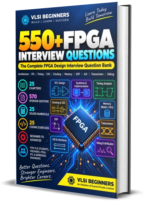
90+ free FPGA questions, from LUTs and RTL coding to timing closure, CDC, memories, AXI and lab debugging. Includes 18 worked answers with code, 8 solved numericals, a timing-report walkthrough and a FIFO depth calculator.
570 questions with interview-ready answers and tips, 25 coding exercises with solutions, 25 solved numericals and 30 debugging scenarios.
FPGA interviews are practical. Beyond "what is a LUT?", you'll be asked to write RTL on a whiteboard, explain why a design fails timing, pick a CDC technique, size a FIFO, or say why a board works in simulation but not in the lab.
This page is built around that. Start with the formula sheet and the FIFO calculator, browse 50 questions across ten topics, then work through the worked answers, numericals and the timing-report walkthrough. Try each one aloud, or on paper for the coding ones, before opening the answer.
LUTs, flops, BRAM and DSP, blocking vs non-blocking, latches, resets, then a short coding task: a synchroniser, a clock enable, an FSM or a counter, written on paper or a shared editor.
MMCM/PLL settings, async FIFOs, BRAM sizing, fixed point, XDC constraints and timing closure, often with a quick calculation like FIFO depth or fmax.
"Works in simulation, not on the board", "the bug vanishes with an ILA", "design a video pipeline". They're testing your method and your trade-offs.
Every line of RTL becomes LUTs, flops, BRAM or DSP. Say what your code infers; that's what interviewers are really checking.
Slow logic runs on the main clock with an enable. Real clocks come from MMCMs/PLLs on global buffers. Saying this unprompted is a strong signal.
When timing fails, check clocks, clock groups, exceptions and I/O delays before touching RTL. Many violations are constraint bugs.
Single bit: two-flop synchroniser. Pulse: toggle synchroniser. Occasional words: handshake. Streams: async FIFO. Counters: Gray code.
Bandwidth, FIFO depth, BRAM count, fmax. A quick, correct number with units makes any design answer more convincing.
Right bitstream? Clocks running, MMCMs locked? Reset released? Pins correct? Then timing, CDC and logic. Most "nothing works" cases are setup issues.
The calculations that come up in FPGA design rounds and real design reviews.
A burst is written at the write clock while the reader drains it. Values update as you type.
| STORAGE | SIZE | READ | BEST FOR | WATCH OUT |
|---|---|---|---|---|
| Flip-flops | Bits | Immediate | Control, pipelines | No bulk storage |
| Distributed (LUT) RAM | Up to a few hundred deep | Asynchronous | Small RAMs, register files | Uses LUTs |
| SRL shift register | 16–32 per LUT | Tap select | Delay lines | No reset |
| Block RAM | 18–36 Kb (M20K: 20 Kb) | Synchronous | FIFOs, buffers | 1–2 cycle latency |
| UltraRAM-type | ~288 Kb | Synchronous | Large on-chip buffers | Fewer configurations |
| External DDR / HBM | GB | High latency | Frame buffers, big data | Efficiency, calibration |
A sample of what interviewers draw from most. The full 570-question ebook covers each topic in much more depth, with every question answered.
What's inside the device and how logic maps onto it.
Writing HDL that becomes the hardware you meant.
# delays in synthesizable code (and when are initial values fine on FPGAs)?Control logic, pipelines and flow control.
From RTL to bitstream.
keep, dont_touch and max_fanout attributes for?XDC/SDC and making the design meet its clocks.
create_clock for a 125 MHz input. Do MMCM output clocks need constraints?set_clock_groups -asynchronous?The source of most hard-to-find FPGA bugs.
ASYNC_REG for?Block RAM, FIFOs, multipliers and fixed point.
Getting data on and off the chip.
Proving it works, in simulation and on the board.
Processors, high-level synthesis and power.
PIPELINE II=1 directive ask for?570 questions across 25 chapters, all answered: 25 coding exercises with solutions, 25 solved numericals, 30 debugging scenarios, plus transceivers, SoC FPGAs, security and partial reconfiguration.
Try each one out loud (or on paper for the coding ones) first, then open it. Every answer shows what a strong reply covers, what the interviewer is really listening for, and the mistake that costs candidates the most.
An FPGA is a chip of programmable resources: LUTs and flip-flops for logic, block RAM, DSP slices, clock managers, I/O and often transceivers and hard processors, connected by programmable routing. A bitstream configures them into your design.
FPGAs win for low-to-medium volume, evolving standards, prototyping and anything that must be reprogrammed. ASICs win at high volume or tight power and performance targets.
A k-input LUT is a tiny 2k-bit memory. The inputs form the address and the stored bits are the truth table, so a LUT6 can implement any function of six inputs with the same delay. Wider functions are built from several LUTs in levels, which is why "logic levels" matter for timing.
Arithmetic would be slow in LUTs alone, because a carry has to ripple through general routing. The dedicated carry chain runs vertically through the logic blocks with fast, fixed connections, so adders, counters and comparators are much faster.
Many LUT6s can also be split into two smaller LUTs sharing inputs, or used as 64-bit distributed RAM or a 32-bit shift register (SRL).
A blocking assignment (=) updates immediately, so later statements in the same block see the new value. A non-blocking assignment (<=) schedules the update for the end of the time step, so every right-hand side uses the old value, just as flops all update together on the edge.
// Wrong: collapses to one stage in simulation always_ff @(posedge clk) begin b = a; c = b; end // Right: two real stages always_ff @(posedge clk) begin b <= a; c <= b; end
The blocking version can also simulate differently from what synthesis builds, a simulation/synthesis mismatch.
In a combinational block, if a signal isn't assigned on every path (an if without else, a case without default), the tool must remember its old value, so it builds a latch.
always_comb begin y = '0; // default first: no latch possible if (sel) y = a; end
Latches are bad in FPGAs: they're built from LUT feedback or used as latch-mode registers, they make timing analysis harder, and they're almost always unintended. Use always_comb, assign defaults at the top, and read the synthesis log for latch warnings.
The common rule is assert asynchronously, de-assert synchronously: pass the reset through a reset synchroniser in each clock domain so release is aligned to that domain's clock.
Equally important: don't reset what doesn't need it. Datapath registers that are overwritten anyway can skip reset, which cuts fanout, frees routing and lets the tool use SRLs and DSP pipeline registers.
A clock generated in logic (a flop toggling, a gate on the clock) doesn't use the dedicated low-skew global clock network. It adds skew, can glitch, and creates a new clock domain that needs its own constraints and CDC.
logic tick; always_ff @(posedge clk) tick <= ~tick; // every 2nd cycle always_ff @(posedge clk) if (tick) q <= d; // slow logic, same clock
The slow logic still runs on the main clock, so it's one domain and fully timed. If you need a real second frequency, make it with an MMCM/PLL or a clock-buffer divider so it sits on a global clock network and the tool knows its relationship to the source.
(* ASYNC_REG = "TRUE" *) logic s1, s2; always_ff @(posedge clk_dst) begin s1 <= async_in; // may go metastable s2 <= s1; // has a full cycle to resolve end
The first flop may go metastable, but it has almost a whole destination clock period to resolve before the second flop samples it, so the chance of a bad value reaching the logic becomes tiny.
MTBF = etr/τ / (T0 · fclk · fdata). Resolution time is in the exponent, so it matters most: keep the two flops close together with no logic between them (that's what ASYNC_REG asks the tool to do), and add a third stage for very fast clocks.
Because the synchronised pointers are a few cycles late, the flags are pessimistic (full and empty may stay asserted a little long) but never wrong. Constrain the pointer crossings with set_max_delay -datapath_only rather than a plain false path.
create_clock -name sys_clk -period 8.000 [get_ports sys_clk_p]
# MMCM outputs are derived automatically from the input clock
set_clock_groups -asynchronous \
-group [get_clocks -include_generated_clocks sys_clk] \
-group [get_clocks -include_generated_clocks eth_rxclk]
set_input_delay -clock eth_rxclk -max 2.0 [get_ports {rxd[*]}]
set_input_delay -clock eth_rxclk -min 0.5 [get_ports {rxd[*]}]
set_max_delay -datapath_only 4.0 -from [get_cells wr_gray_reg*] -to [get_cells rd_sync1_reg*]Then check the report for unconstrained paths and clock-interaction warnings.
max_fanout or physical optimisation).logic [31:0] mem [0:4095]; always_ff @(posedge clk) begin if (we) mem[waddr] <= wdata; rdata <= mem[raddr]; // registered read → block RAM end
A registered (synchronous) read is what lets the tool map to BRAM. An asynchronous read, or a reset on the memory array, forces LUT RAM or flops.
Every AXI channel transfers on the clock edge where both VALID (from the source) and READY (from the destination) are high.
AXI4 has five independent channels (write address, write data, write response, read address, read data). AXI4-Lite drops bursts for simple register access; AXI4-Stream has no addresses, just a data stream with TVALID/TREADY and TLAST.
In long pipelines a combinational READY becomes a timing problem; a skid buffer registers READY and holds the in-flight word in a second register.
Routing-dominated paths with huge fanout aren't a logic-depth problem. One register drives cells spread across the die, so the net is long and slow.
max_fanout on the register, or let physical optimisation duplicate it near its loads.See the timing report walkthrough below for exactly this path.
Same bitstream, different result means the design has no margin somewhere, and part-to-part or board-to-board variation pushes one unit over the edge:
Swap parts between boards, vary temperature and voltage, and check timing and CDC reports for unconstrained paths.
Adding the ILA changed placement and routing, and the bug went away. That points to timing or CDC sensitivity, not a logic error: a path or crossing that works or fails depending on where things land.
At that utilization, routing congestion makes almost every path slow. Free up resources before fighting individual paths:
FPGA interviews often include quick sizing and timing calculations. Work each one on paper first, then tap to check.
Tmin = 0.30 + 1.00 + 1.90 + 0.05 + 0.08 = 3.33 ns fmax = 1 / 3.33 ns ≈ 300 MHz
Note: routing is 57% of the path, so placement and fanout are the first things to look at.
Before: 6.0 + 0.4 = 6.4 ns → 156 MHz, latency 6.4 ns After : 2.0 + 0.4 = 2.4 ns → 417 MHz Speed-up ≈ 2.67× (not 3×), latency 3 × 2.4 = 7.2 ns
Note: register overhead is paid in every stage, and total latency goes up. Always mention both.
M = 10, D = 1 → VCO = 100 × 10 / 1 = 1,000 MHz (in range) O1 = 1,000 / 250 = 4 → 250 MHz O2 = 1,000 / 125 = 8 → 125 MHz
Note: both outputs share one VCO, so they're related clocks with a known phase relationship.
Burst time = 800 / 200 MHz = 4.0 µs Words read = 4.0 µs × 150 MHz = 600 Depth ≥ 800 − 600 = 200 → choose 256
Note: 256 leaves 56 words of margin for synchroniser latency and read start-up. These are the default values in the calculator above.
A 36 Kb BRAM can be 2K × 18 (or 4K × 9, 8K × 4 …) Width: 16 bits fits one 2K × 18 block Depth: 8,192 / 2,048 = 4 → 4 BRAMs
Note: 2 bits per word go unused. Shapes that match the BRAM aspect ratios waste nothing.
0.5 → 0x4000 (16,384) 0.25 → 0x2000 (8,192) Q1.15 × Q1.15 = Q2.30, 32 bits 16,384 × 8,192 = 134,217,728 = 0x0800_0000 ÷ 2^30 = 0.125 Back to Q1.15: shift right 15 → 4,096 = 0x1000 = 0.125
Note: when going back, round instead of truncating and saturate on overflow.
AXI-Stream: 128 × 250 MHz = 32 Gb/s = 4 GB/s (TVALID and TREADY always high) DDR4-3200 ×32: 3,200 MT/s × 4 B = 12.8 GB/s peak At ~70%: ≈ 9.0 GB/s
Note: DDR efficiency depends on access patterns: refresh, row misses and read/write turnarounds.
Divider = 50,000,000 / (16 × 9,600) = 325.5 → 326 Actual = 50,000,000 / (16 × 326) ≈ 9,586 baud Error ≈ −0.15%
Note: UARTs tolerate roughly ±2–3% total, so this is fine. A fractional divider helps when it isn't.
"Here's the worst path. What would you do?" is a standard FPGA question. This path fails because of routing and fanout, not logic depth. Generic vendor-style format, units in ns.
Slack (VIOLATED) : -0.370ns (required time - arrival time) Source: u_ctrl/acc_en_reg/C (rising edge-triggered cell FDRE clocked by clk_250) Destination: u_dsp/acc_reg[31]/CE (rising edge-triggered cell FDRE clocked by clk_250) Path Group: clk_250 Path Type: Setup (Max at Slow Process Corner) Requirement: 4.000ns (clk_250 rise@4.000ns - clk_250 rise@0.000ns) (1) Data Path Delay: 4.200ns (logic 1.350ns (32.1%) route 2.850ns (67.9%)) (2) Logic Levels: 5 (CARRY8=1 LUT6=4) Clock Path Skew: -0.040ns (3) Clock Uncertainty: 0.070ns Location Delay type Incr(ns) Netlist Resource(s) --------------------------------------------------------------- SLICE_X40 FDRE (Prop_C_Q) 0.450 u_ctrl/acc_en_reg/Q net (fo=1240, routed) 1.320 u_ctrl/acc_en (4) SLICE_X88 LUT6 (Prop_I0_O) 0.120 u_dsp/sel_i_1/O net (fo=3, routed) 0.380 SLICE_X89 LUT6 (Prop_I2_O) 0.150 u_dsp/sum_i_7/O net (fo=1, routed) 0.410 SLICE_X90 CARRY8 (Prop_S_CO) 0.380 u_dsp/cmp_carry/CO net (fo=2, routed) 0.290 SLICE_X91 LUT6 (Prop_I3_O) 0.120 u_dsp/ce_i_2/O net (fo=1, routed) 0.250 SLICE_X92 LUT6 (Prop_I1_O) 0.130 u_dsp/ce_i_1/O net (fo=32, routed) 0.200 u_dsp/acc_ce SLICE_X93 FDRE u_dsp/acc_reg[31]/CE --------------------------------------------------------------- Arrival = 4.200ns Required = 4.000 - 0.040 - 0.070 - 0.060 (setup) = 3.830ns Slack = 3.830 - 4.200 = -0.370ns (5)
A single enable register drives 1,240 loads spread across the device, so its net alone takes 1.32 ns, and the remaining routing between five levels of logic uses up the rest of the 4 ns budget.
Replicate acc_en_reg so each copy drives a local group of loads (max_fanout on the register, or physical-optimisation replication). If the logic allows one more cycle of latency, register the enable once more near the DSP block. Either one removes most of the 1.32 ns.
Maybe partly, but it's the wrong first move. The report shows a structural cause, fanout, that will keep coming back as the design changes. Fix the structure, then use strategies for the last few tens of picoseconds.
Whether other failing paths share the same source (one fix may clear many), whether acc_en is really a reset-like signal that half its loads don't need, and whether the DSP accumulator is using the DSP slice's internal pipeline registers. The ebook covers report_timing_summary and closure in two full chapters.
Screening rounds often open with fast checks like these. Aim to answer each in under ten seconds, then tap to check.
Any function of 6 inputs: 264 of them.
Non-blocking (<=).
A signal not assigned on every path in a combinational block.
For SRAM-based FPGAs, yes: it reloads from flash at power-up.
One-hot is usually faster: flops are plentiful and next-state logic is simpler.
A registered (synchronous) read, and no reset on the array.
A LUT used as a 16–32-bit shift register.
Marks synchroniser flops so they're placed together and analysed for MTBF.
Only one bit changes per increment, so a mid-change sample is still valid.
Toggle synchroniser: toggle a flop, synchronise it, edge-detect on the other side.
FVCO = Fin × M / D, kept inside the allowed range.
set_clock_groups -asynchronous, with real CDC in the RTL.
Q2.30, 32 bits.
log264 = 6.
80%.
On a clock edge where VALID and READY are both high.
An integrated logic analyser: on-chip capture of internal signals, viewed over JTAG.
A new input is accepted every clock cycle.
Voltage (V2), then switching activity: clock gating and enables.
The constraints.
Interviewers often use their own vendor's terms. Know the equivalents so you can map your experience to theirs.
| CONCEPT | AMD / XILINX | INTEL / ALTERA |
|---|---|---|
| Basic logic element | LUT6 + flip-flops in a slice / CLB | ALM (fracturable LUT + registers) in a LAB |
| Block memory | Block RAM (18 / 36 Kb), UltraRAM | M20K (20 Kb), plus larger blocks on some families |
| Multiplier block | DSP48 / DSP58 slice (27 × 18 class) | Variable-precision DSP block (27 × 27 or two 18 × 19) |
| Clock synthesis | MMCM, PLL | IOPLL, fPLL |
| Global clock buffer | BUFG / BUFGCE | Global / regional clock networks (clock control block) |
| Constraints | XDC (SDC-based Tcl) | SDC, plus QSF for assignments |
| Design tool | Vivado (Vitis for software/HLS) | Quartus Prime |
| On-chip logic analyser | ILA (with VIO for control) | Signal Tap (with In-System Sources and Probes) |
Loops that can't unroll, sequential thinking in combinational blocks, and no idea what the code infers. Always say what each block becomes.
Using a counter bit or a gated signal as a clock. Use a clock enable, or an MMCM/PLL for a real new frequency.
Two-flop synchronisers are for single bits. Multi-bit values need Gray code, a handshake or an async FIFO.
It makes the report clean and hides real problems. Use clock groups for truly async clocks and bounded max-delays for CDC buses.
Resetting every datapath register creates huge fanout nets, blocks SRL and DSP inference, and hurts timing.
Most "nothing works on the board" problems are the wrong bitstream, a clock not locked, reset held, or a pin assignment. Check those first.
Usually two or three: a fundamentals and RTL coding round, a design round on clocking, CDC, memories, timing and interfaces, and for experienced candidates a debugging or system-design round.
Almost always. Common tasks are a synchroniser, a clock enable instead of a divided clock, a counter or PWM, an FSM, a debouncer, a Gray converter or a small FIFO. Write synthesizable code with non-blocking assignments in clocked blocks. Practise with our Verilog questions.
No. Know one tool flow well and the equivalent terms in the other. Concepts such as LUT mapping, BRAM inference, timing constraints and CDC transfer across vendors; interviewers care more about the concepts than the tool names.
Yes. FPGA roles exist in telecom, defence, test and measurement, data centres, automotive, video and ASIC prototyping. The work is hands-on, combining RTL, timing, lab bring-up and often embedded software, and many engineers move between FPGA and ASIC.
Learn FPGA architecture (LUTs, flip-flops, BRAM, DSP), RTL coding rules, FSMs and timing basics first. Practise writing small modules on paper, then learn CDC, BRAM and FIFOs, and basic XDC constraints. Prepare one board project you can explain in detail.
A clock made in fabric logic doesn't use the dedicated low-skew clock network, so it adds skew, can glitch and creates a new clock domain. Use a clock enable on the original clock, or generate real clocks with an MMCM/PLL.
Book a 1:1 mock interview with a mentor working in this exact domain.
Book a mock interview