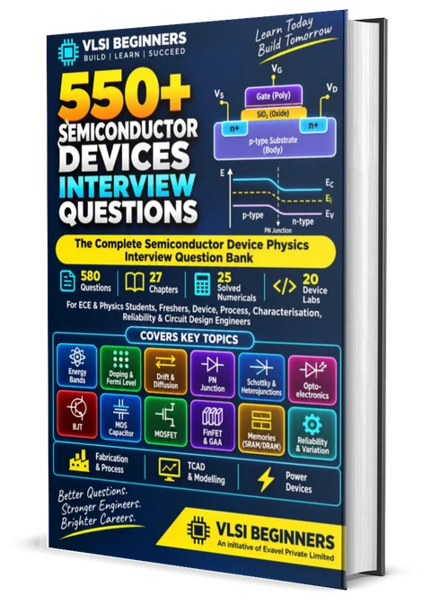
Energy bands to FinFETs, power devices and reliability, in 27 chapters. Each answer gives the physical picture an interviewer wants to hear, plus a tip on what they'll probe next. Includes 20 Python and SPICE device labs, 25 solved numericals and 30 fab and lab debugging scenarios.
Semiconductor questions test whether you understand what's happening inside the silicon. They decide device, process, characterisation and reliability interviews, and appear in circuit and memory rounds whenever leakage, breakdown or ageing comes up.
Reciting the diode equation isn't enough. Interviewers ask you to draw the band diagram, say where the Fermi level sits and why, explain why the current rises 10× every 60 mV, tell Zener from avalanche by temperature, read a C–V curve, or work out why an NMOS lot came in 80 mV low.
The book builds the subject the way a device engineer learns it: carriers and bands, then junctions and contacts, then transistors and power devices, then memories, reliability, process and modelling, and finally the interview itself.
A device round checks four things: can you explain the physics, sketch the diagram, run the numbers and diagnose real data? Each has its own part of the book.
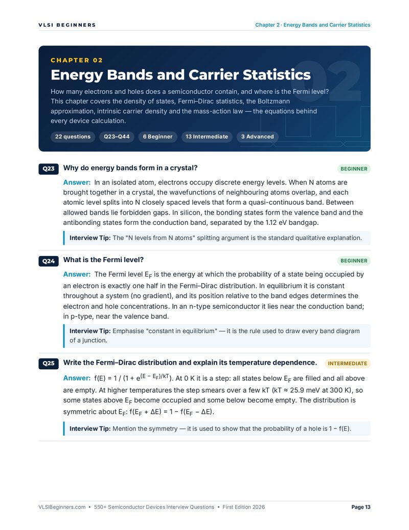
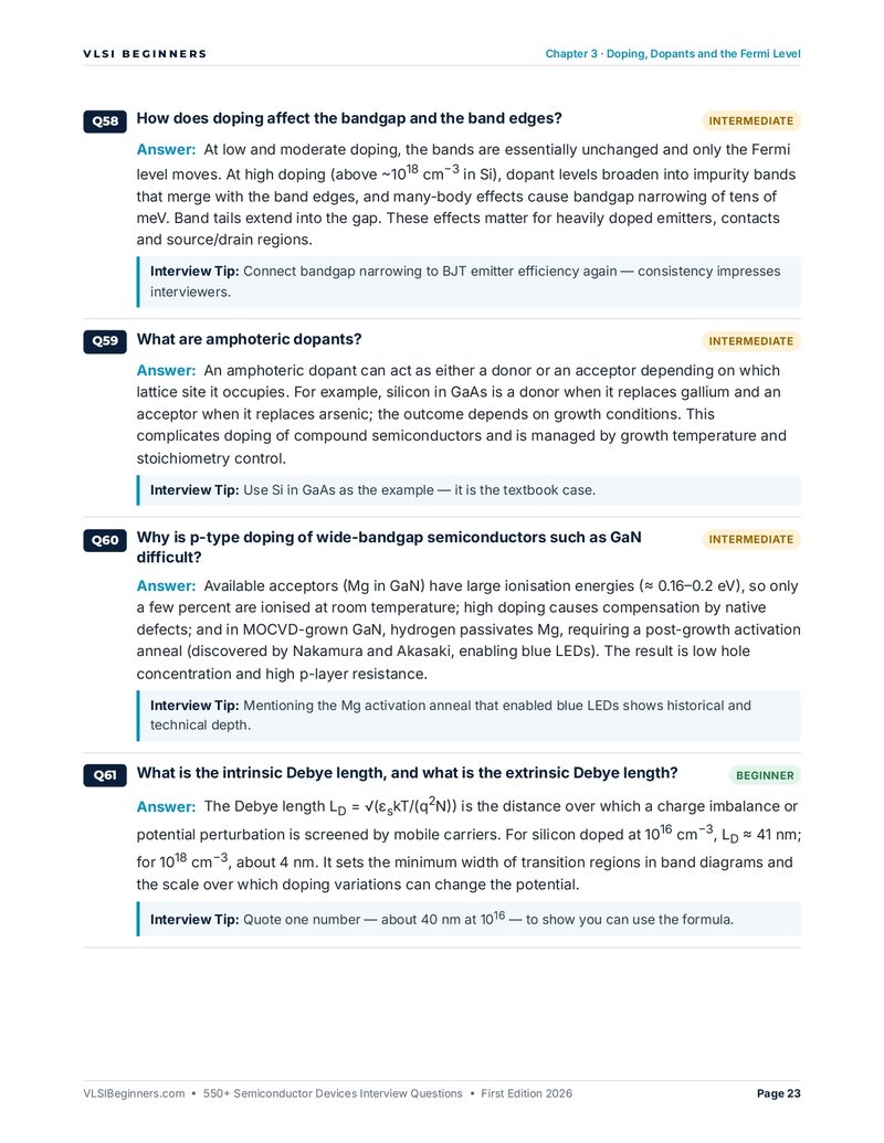
Questions are tagged Beginner, Intermediate or Advanced. Each gets a clear spoken-style answer and an Interview Tip: the analogy, number or follow-up that makes the answer stick.
ni(T), Fermi level and compensation, mobility models, junction electrostatics, a numerical Poisson solver, 1/C2 doping extraction, diode, MOSFET and BJT parameter extraction, Hall data and Weibull fitting.
Carrier densities, Fermi-level position, resistivity, built-in potential, depletion width, diode current, breakdown, Schottky barriers, BJT gain, MOS threshold, body effect, subthreshold leakage and more.
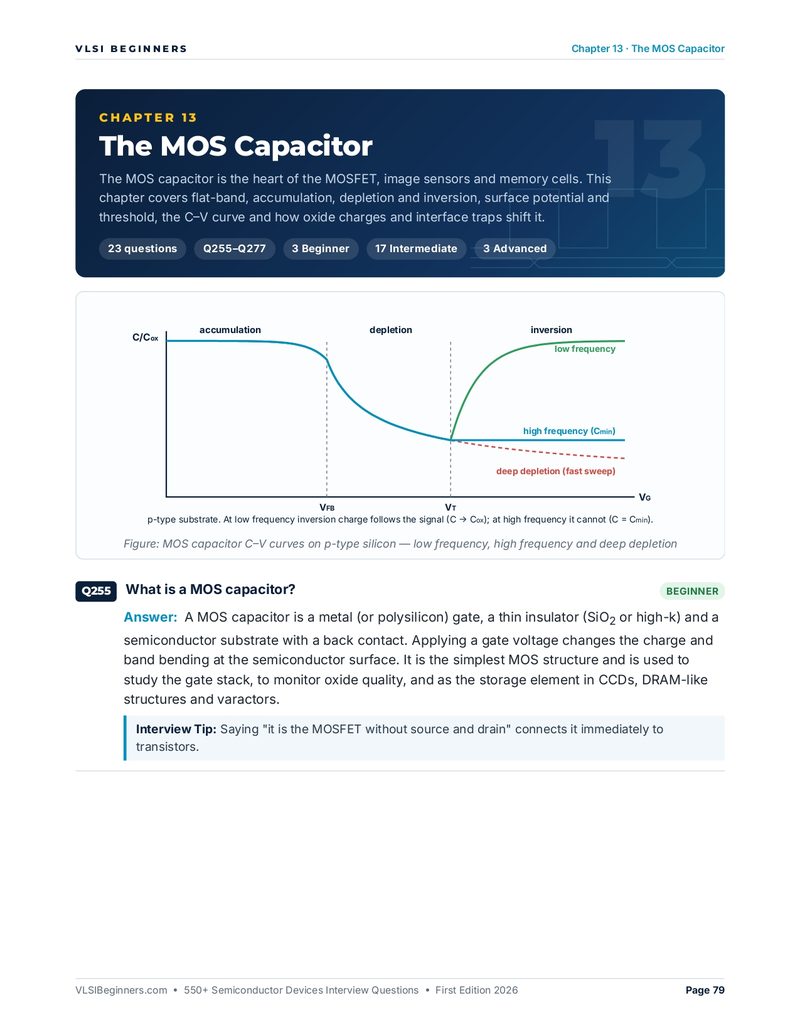
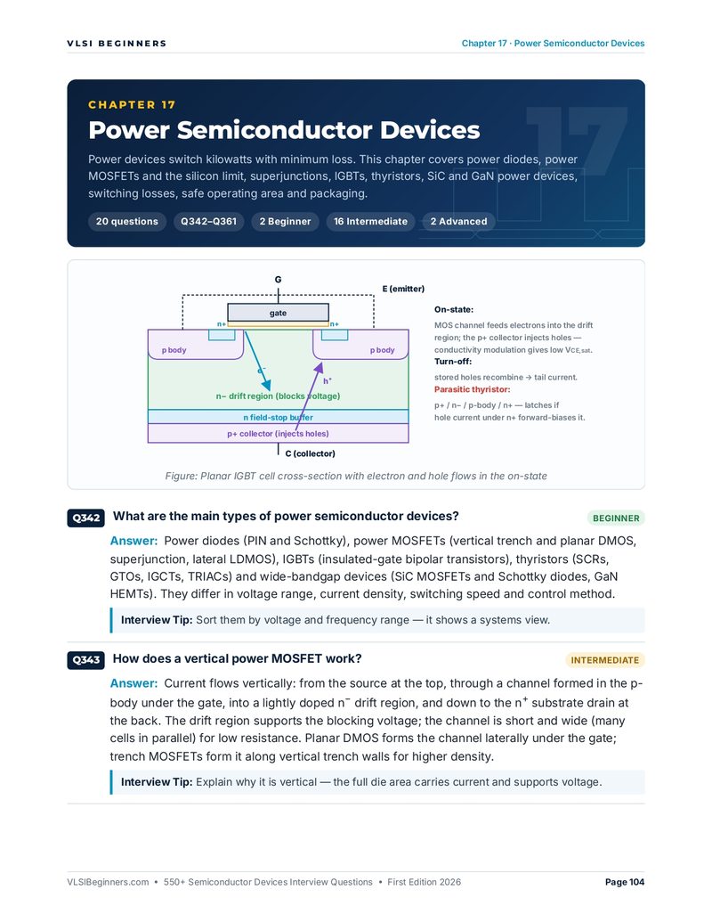
Band diagrams, the MOS C–V curve at low and high frequency, an IGBT cross-section with carrier flows, and an annotated device characterisation report read line by line.
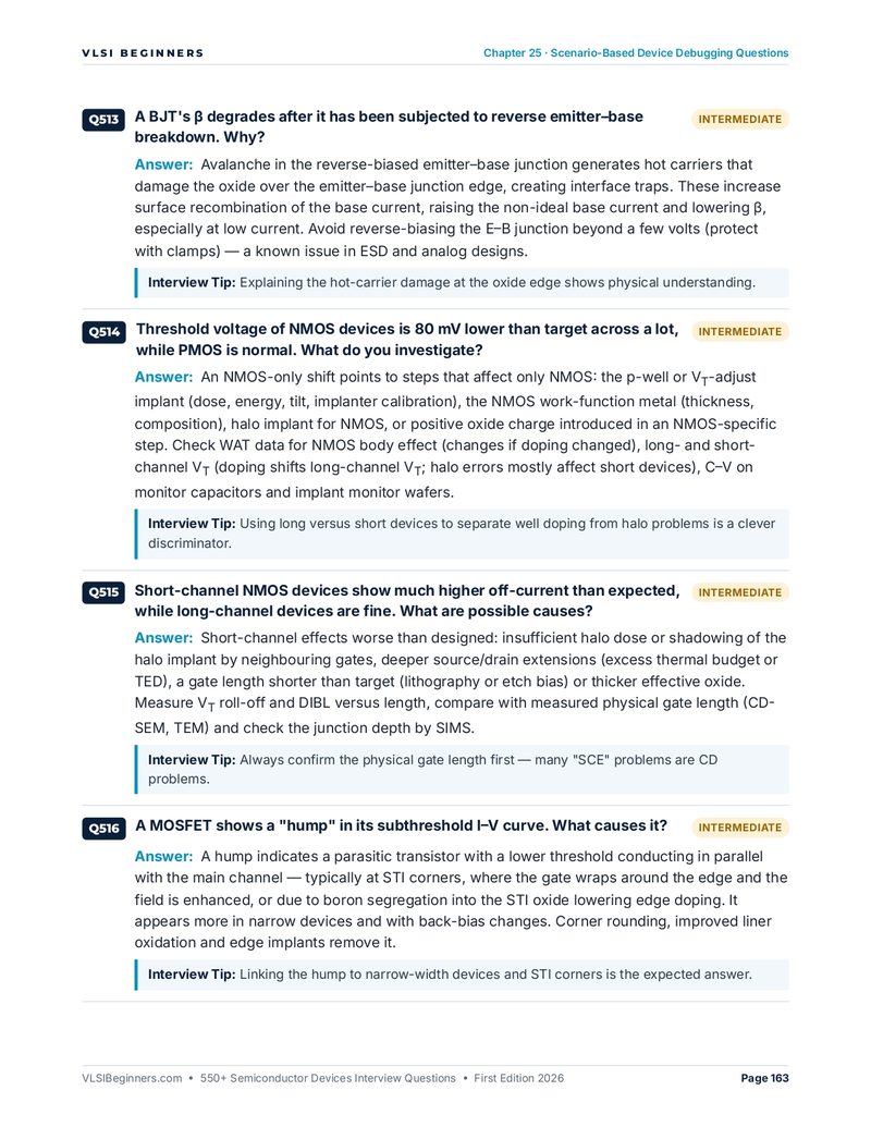
Diode leakage 10× over spec, Zener versus avalanche, BJT gain lost after E–B breakdown, a low-VT NMOS lot, subthreshold humps, wafer-edge shifts, GaN and SiC field issues and flash retention failures.
A formula sheet and key constants, a device selection guide, a 30-question rapid-fire round, a glossary of device terms, a 7-day plan and a readiness checklist.
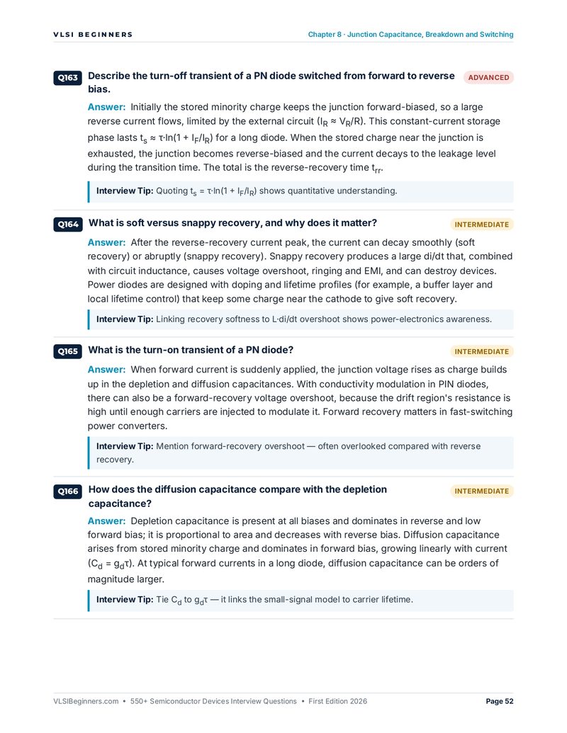
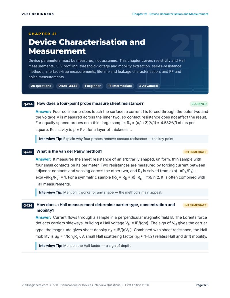
Real pages from the PDF, not mock-ups. Tap any page to open it full size.
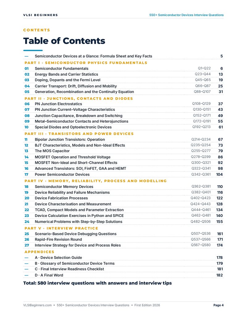
First the carriers, then the junctions they form, then the transistors and power devices built from those junctions. After that come the questions industry asks about memories, reliability, process and models, and finally practice under interview conditions.
| # | CHAPTER | QUESTIONS |
|---|---|---|
| PART I · SEMICONDUCTOR PHYSICS FUNDAMENTALS | ||
| 01 | Semiconductor Fundamentals | Q1–Q22 |
| 02 | Energy Bands and Carrier Statistics | Q23–Q44 |
| 03 | Doping, Dopants and the Fermi Level | Q45–Q65 |
| 04 | Carrier Transport: Drift, Diffusion and Mobility | Q66–Q87 |
| 05 | Generation, Recombination and the Continuity Equation | Q88–Q107 |
| PART II · JUNCTIONS, CONTACTS AND DIODES | ||
| 06 | PN Junction Electrostatics | Q108–Q129 |
| 07 | PN Junction Current–Voltage Characteristics | Q130–Q151 |
| 08 | Junction Capacitance, Breakdown and Switching | Q152–Q171 |
| 09 | Metal–Semiconductor Contacts and Heterojunctions | Q172–Q191 |
| 10 | Special Diodes and Optoelectronic Devices | Q192–Q213 |
| PART III · TRANSISTORS AND POWER DEVICES | ||
| 11 | Bipolar Junction Transistors: Operation | Q214–Q234 |
| 12 | BJT Characteristics, Models and Non-Ideal Effects | Q235–Q254 |
| 13 | The MOS Capacitor | Q255–Q277 |
| 14 | MOSFET Operation and Threshold Voltage | Q278–Q299 |
| 15 | MOSFET Non-Ideal and Short-Channel Effects | Q300–Q321 |
| 16 | Advanced Transistors: SOI, FinFET, GAA and HEMT | Q322–Q341 |
| 17 | Power Semiconductor Devices | Q342–Q361 |
| PART IV · MEMORY, RELIABILITY, PROCESS AND MODELLING | ||
| 18 | Semiconductor Memory Devices | Q362–Q381 |
| 19 | Device Reliability and Failure Mechanisms | Q382–Q401 |
| 20 | Device Fabrication Processes | Q402–Q423 |
| 21 | Device Characterisation and Measurement | Q424–Q443 |
| 22 | TCAD, Compact Models and Parameter Extraction | Q444–Q461 |
| 23 | Device Calculation Exercises in Python and SPICE | Q462–Q481 |
| 24 | Numerical Problems with Step-by-Step Solutions | Q482–Q506 |
| PART V · INTERVIEW PRACTICE | ||
| 25 | Scenario-Based Device Debugging Questions | Q507–Q536 |
| 26 | Rapid-Fire Revision Round | Q537–Q566 |
| 27 | Interview Strategy for Device and Process Roles | Q567–Q580 |
| APPENDICES | ||
| A | Device Selection Guide | p. 178 |
| B | Glossary of Semiconductor Device Terms | p. 179 |
| C | Final Interview Readiness Checklist | p. 181 |
| D | A Final Word | p. 182 |
A must-know equation, a strong analogy, a power-device effect, a forward-looking device and a lab diagnosis. All 580 follow the same format: the answer, then the tip that makes it memorable.
Get the ebook nowAnswer aloud before reading. Sketch band diagrams, C–V curves and device cross-sections from memory, solve Chapter 24 on paper, and rerun the Chapter 23 scripts.
Campus drives, M.Tech and PhD interviews and core-company tests. Parts I and II turn semester notes into clear spoken answers.
Fabrication steps, threshold control, short-channel effects, FinFET and GAA, compact models, parameter extraction and wafer-level debugging.
Hall, C–V and four-point probe, extraction methods, BTI, HCI, TDDB, electromigration, Weibull statistics and qualification.
Leakage, breakdown, latch-up, diode recovery, power MOSFETs, IGBTs, SiC and GaN: the device behaviour behind your circuits.
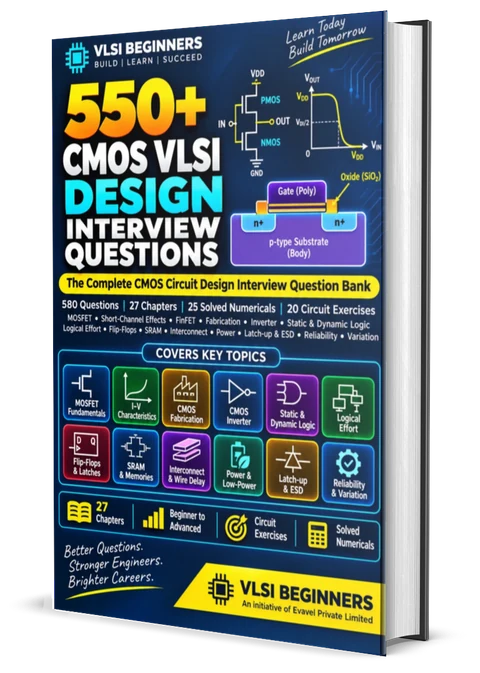
This book explains how a transistor works. The CMOS ebook turns transistors into circuits: 580 answered questions on inverters, logic styles, sizing, SRAM, interconnect, power, latch-up and variation.
580 answered questions in 27 chapters, with device labs, numericals and fab debugging. Download the PDF straight after checkout.
Get the ebook nowYes. Every question has a full answer, phrased the way you would explain it in an interview, plus an interview tip. The 20 device labs include working Python or ngspice code, and the 25 numericals are solved step by step.
A 183-page PDF. Checkout is on Topmate and the download is available right after payment.
Device, process, characterisation, reliability and TCAD roles first, plus circuit, memory and analog design candidates who face a device-physics round. It also suits ECE and physics students preparing for core semiconductor companies and research interviews.
No. Part I starts from crystals, bands and doping, and 120 questions are marked Beginner. Each answer explains the physical picture first and the equation second.
Yes. There are chapters on short-channel effects, SOI, FinFET, gate-all-around and CFET, GaN HEMTs, SiC and IGBT power devices, flash and emerging memories, and reliability mechanisms such as BTI, HCI, TDDB and electromigration.
Yes. Eight real pages are on this page, and the free Semiconductor Interview Questions page has 90+ sample questions with worked answers, solved numericals and a carrier and Fermi-level calculator.
Because this is a digital product delivered instantly, sales are generally final. If you hit a technical issue with your download, contact us within 7 days. See our Refund Policy for details.
Preparing for another round too? Browse all ebooks →