ANALOG & MIXED-SIGNAL INTERVIEW PREP

Draw it, size it, stabilise it. 580 analog VLSI questions, fully answered.

From the MOSFET and gm/ID through mirrors, differential pairs, op-amps, compensation and noise to bandgaps, LDOs, comparators, data converters, PLLs, layout and sign-off, in 27 chapters. Each answer is written the way you'd say it at the whiteboard, with a tip on what the interviewer will probe next. Includes 25 solved numericals, 20 SPICE circuit exercises and 30 debugging scenarios.

186-PAGE PDF · INSTANT DOWNLOAD · 8 FREE PREVIEW PAGES BELOW
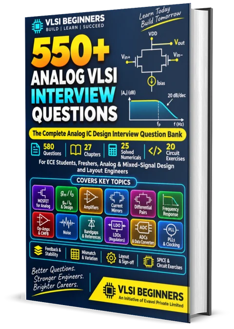
550+ Analog VLSI Interview Questions ebook cover — VLSI Beginners
580
QUESTIONS WITH ANSWERS
27
CHAPTERS IN 5 PARTS
25
SOLVED NUMERICALS
20
SPICE CIRCUIT EXERCISES
THE PROBLEM

Analog interviews test how you think, not what you've memorised

An analog interviewer draws a circuit and starts asking. What's the gain? The output resistance? Where are the poles? What limits the swing? What happens to the noise if you double the current?

Then the follow-ups get harder. Why does this mirror need a cascode? How does one Miller capacitor split two poles? Why does a bandgap need a start-up circuit? Why does kT/C set the size of an ADC's sampling capacitor? Strong answers combine intuition, a short hand calculation and a trade-off.

Good analog material for interviews is hard to find: textbooks go deep but don't tell you what to say, and question lists don't explain. This book is written for the whiteboard: the device first, then amplifiers and feedback, then the building blocks, then layout and sign-off, and finally the interview itself.

WHAT'S INSIDE

From one transistor to a signed-off block

An analog round checks four things: can you analyse a circuit by hand, do you understand the trade-offs, can you design a block to a specification, and can you find out why silicon doesn't match simulation? Each has its own part of the book.

ANSWERS

580 answers, each with a tip

Questions are tagged Beginner, Intermediate or Advanced. Each gets a clear spoken-style answer and an Interview Tip: the number, phrase or follow-up that separates a good answer from a great one.

NUMERICALS

25 solved numericals

gm, ro and intrinsic gain, gm/ID sizing, cascode and mirror errors, OTA gain, GBW and slew, settling time, thermal noise and kT/C, ENOB and jitter, bandgap ratios, LDO dropout, latch time, LC tanks, PLL dividers and Pelgrom mismatch.

SPICE EXERCISES

20 circuit exercises with results

CS and follower stages, cascode mirrors, a five-transistor OTA, a two-stage Miller op-amp with nulling resistor, kT/C noise, constant-gm bias, a bandgap, SC resistors, jitter, SAR mismatch, sigma-delta, ring oscillators and a PLL loop filter.

DIAGRAMS

The circuits interviewers draw

The analog design flow, gm/ID versus inversion, cascode mirrors, the two-stage Miller op-amp, a loop-gain Bode plot, a bandgap, an LDO, an SC gain stage, a SAR ADC, a charge-pump PLL and matching layouts.

DEBUGGING

30 real debugging scenarios

Ringing at the fast corner, an op-amp stuck at a rail, bandgap spread in Monte Carlo, 6 dB lost after layout, ADC spurs, SAR DNL, a PLL that won't lock, an LDO that oscillates at light load and a bandgap that won't start on silicon.

QUICK REVISION

Built for the last day

Key equations at a glance, an annotated characterisation report, a 40-question rapid-fire round, rules of thumb, a glossary, a 7-day plan, interview strategy and a final readiness checklist.

LOOK INSIDE

Eight pages, straight from the book

Real pages from the PDF, not mock-ups. Tap any page to open it full size.

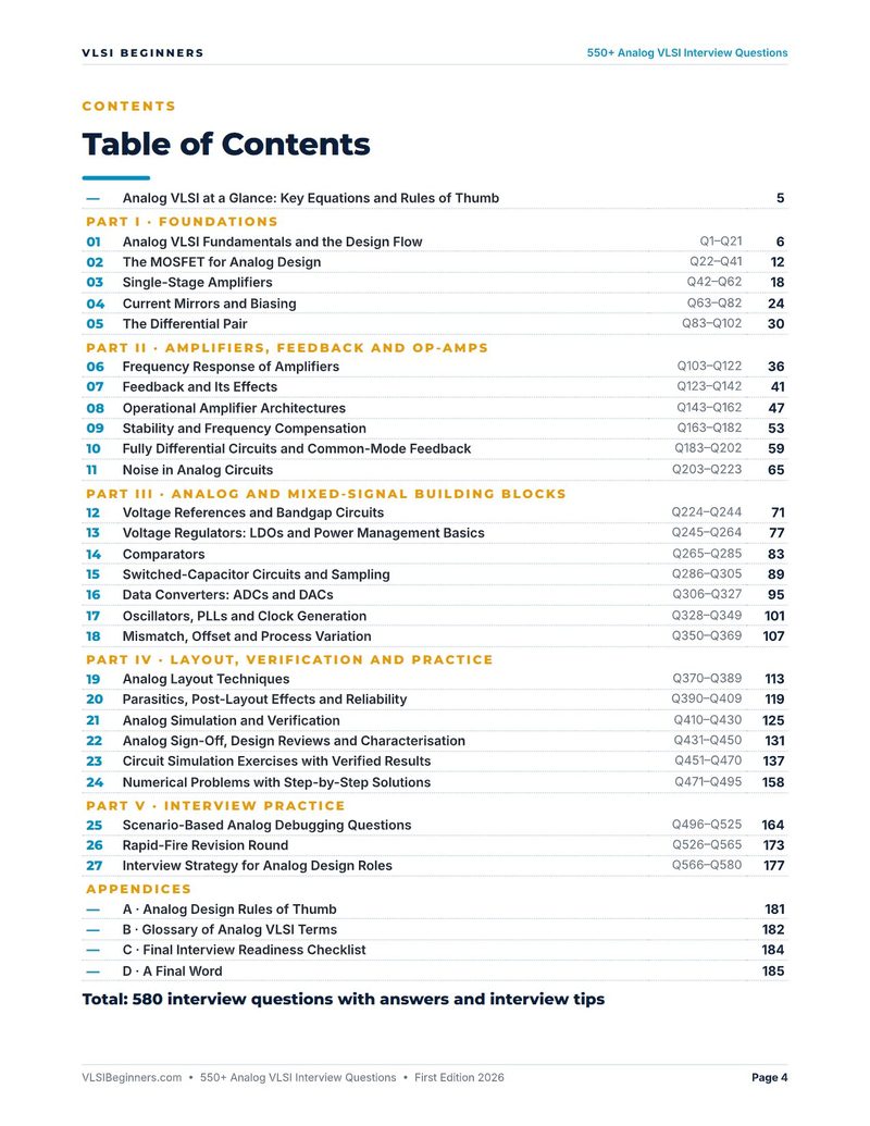
Table of contents listing 27 chapters in five parts with question ranges, plus four appendices
PAGE 4Contents and question ranges
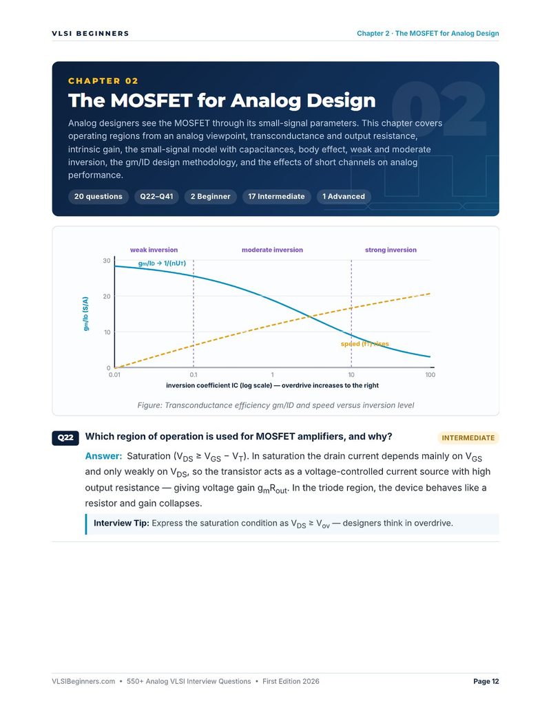
Chapter 2 opener with a plot of gm/ID and speed against inversion level, and the first question on operating regions
CHAPTER 2gm/ID and inversion
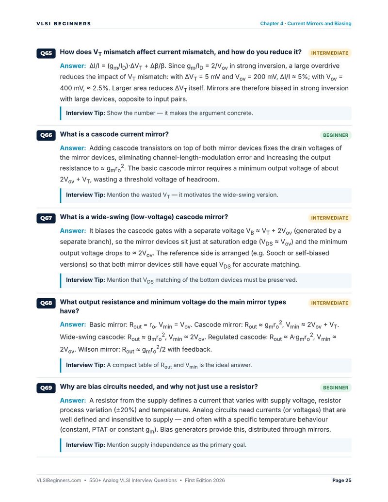
Chapter 4 page on VT mismatch in mirrors, cascode and wide-swing cascode mirrors, mirror output resistance and bias circuits
CHAPTER 4Cascode mirrors
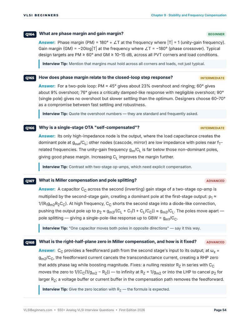
Chapter 9 page on phase and gain margin, overshoot versus phase margin, self-compensated OTAs, Miller compensation and the RHP zero
CHAPTER 9Miller compensation
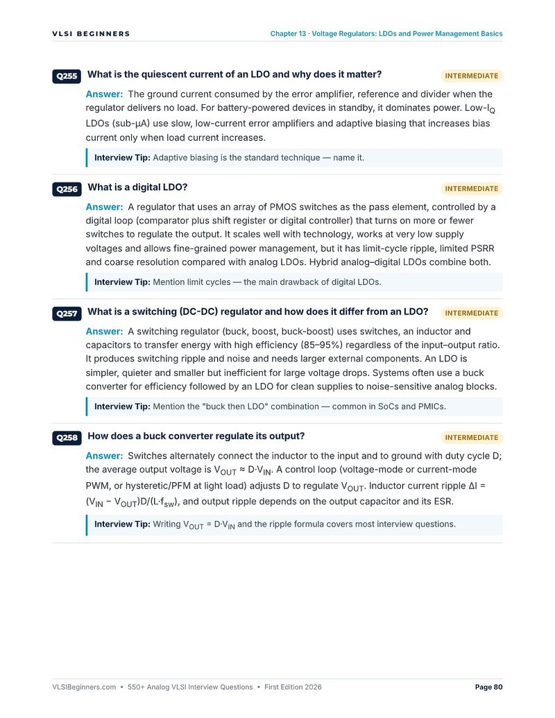
Chapter 13 page on LDO quiescent current, digital LDOs and how switching regulators compare with LDOs
CHAPTER 13LDOs and DC-DC
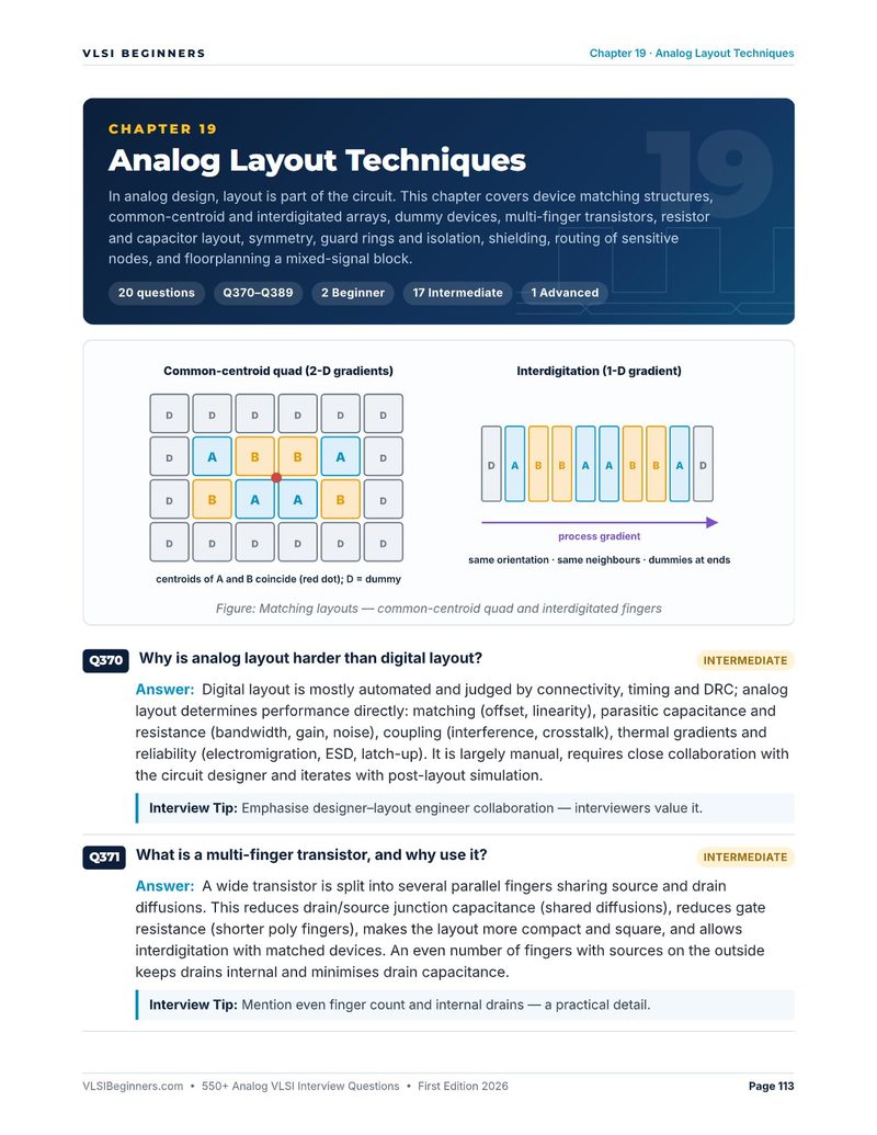
Chapter 19 opener with common-centroid and interdigitated matching layouts, and questions on analog layout and multi-finger devices
CHAPTER 19Matching layouts
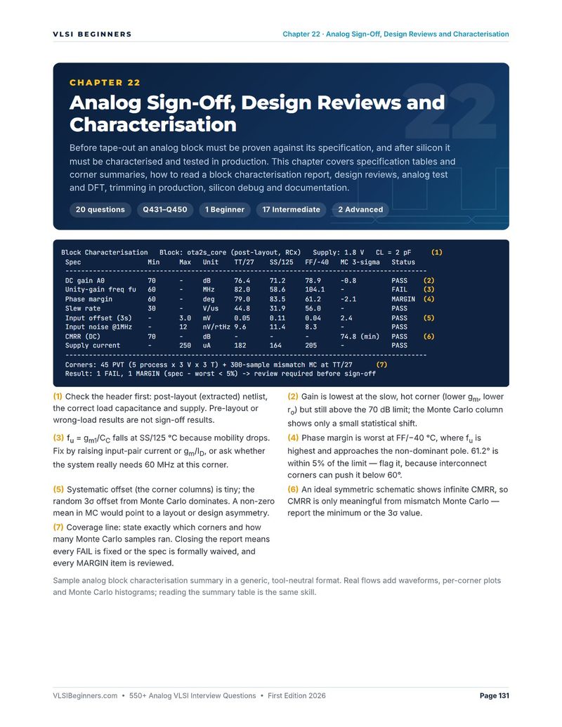
Chapter 22 opener with an annotated op-amp characterisation report across PVT corners and Monte Carlo
CHAPTER 22Annotated sign-off report
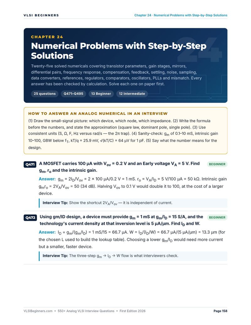
Chapter 24 opener with a method for answering analog numericals and two solved problems on gm, ro and gm/ID sizing
CHAPTER 24Solved numericals
HOW IT'S STRUCTURED

Five parts, from the device to the interview

First the transistor and the basic stages built from it, then frequency response, feedback, op-amps and noise. After that come the mixed-signal building blocks and mismatch, then layout, verification and sign-off with exercises and numericals, and finally debugging under interview conditions.

PART I — FOUNDATIONS
The device and the basic stages
CH 1–5The analog design flow, the MOSFET for analog design and gm/ID, single-stage amplifiers, current mirrors and biasing, the differential pair
102QUESTIONS
PART II — AMPLIFIERS, FEEDBACK & OP-AMPS
Gain, bandwidth, stability and noise
CH 6–11Frequency response, feedback, op-amp architectures, stability and compensation, fully differential circuits and CMFB, noise
121QUESTIONS
PART III — ANALOG & MIXED-SIGNAL BLOCKS
The blocks every SoC needs
CH 12–18Bandgap references, LDOs and power management, comparators, switched-capacitor circuits, ADCs and DACs, oscillators and PLLs, mismatch and process variation
146QUESTIONS
PART IV — LAYOUT, VERIFICATION & PRACTICE
From schematic to signed-off silicon
CH 19–24Analog layout, parasitics and reliability, simulation and verification, sign-off and characterisation, 20 SPICE exercises with verified results, 25 solved numericals
126QUESTIONS
PART V — INTERVIEW PRACTICE
Answering under pressure
CH 25–2730 scenario-based debugging questions, a 40-question rapid-fire round, and interview strategy for analog design roles
85QUESTIONS
TOTAL ACROSS 27 CHAPTERS + 4 APPENDICES 580 questions
DIFFICULTY SPLIT
120 Beginner: concepts every candidate must know405 Intermediate: hand analysis and design trade-offs55 Advanced: compensation, silicon and senior depth
SEE ALL 27 CHAPTERS
#CHAPTERQUESTIONS
PART I · FOUNDATIONS
01Analog VLSI Fundamentals and the Design FlowQ1–Q21
02The MOSFET for Analog DesignQ22–Q41
03Single-Stage AmplifiersQ42–Q62
04Current Mirrors and BiasingQ63–Q82
05The Differential PairQ83–Q102
PART II · AMPLIFIERS, FEEDBACK AND OP-AMPS
06Frequency Response of AmplifiersQ103–Q122
07Feedback and Its EffectsQ123–Q142
08Operational Amplifier ArchitecturesQ143–Q162
09Stability and Frequency CompensationQ163–Q182
10Fully Differential Circuits and Common-Mode FeedbackQ183–Q202
11Noise in Analog CircuitsQ203–Q223
PART III · ANALOG AND MIXED-SIGNAL BUILDING BLOCKS
12Voltage References and Bandgap CircuitsQ224–Q244
13Voltage Regulators: LDOs and Power Management BasicsQ245–Q264
14ComparatorsQ265–Q285
15Switched-Capacitor Circuits and SamplingQ286–Q305
16Data Converters: ADCs and DACsQ306–Q327
17Oscillators, PLLs and Clock GenerationQ328–Q349
18Mismatch, Offset and Process VariationQ350–Q369
PART IV · LAYOUT, VERIFICATION AND PRACTICE
19Analog Layout TechniquesQ370–Q389
20Parasitics, Post-Layout Effects and ReliabilityQ390–Q409
21Analog Simulation and VerificationQ410–Q430
22Analog Sign-Off, Design Reviews and CharacterisationQ431–Q450
23Circuit Simulation Exercises with Verified ResultsQ451–Q470
24Numerical Problems with Step-by-Step SolutionsQ471–Q495
PART V · INTERVIEW PRACTICE
25Scenario-Based Analog Debugging QuestionsQ496–Q525
26Rapid-Fire Revision RoundQ526–Q565
27Interview Strategy for Analog Design RolesQ566–Q580
APPENDICES
AAnalog Design Rules of Thumbp. 181
BGlossary of Analog VLSI Termsp. 182
CFinal Interview Readiness Checklistp. 184
DA Final Wordp. 185
FROM THE BOOK

Five questions, unedited

A mirror every candidate must explain, a two-minute numerical, the stability basics, a senior-level compensation question and a power-management comparison. All 580 follow the same format: the answer, then the tip that makes it stick.

Get the ebook now
Q66BEGINNER · CURRENT MIRRORS What is a cascode current mirror? Adding cascode transistors on top of both mirror devices fixes the drain voltages of the mirror devices, eliminating channel-length-modulation error and increasing the output resistance to ≈ gmro2. The basic cascode mirror requires a minimum output voltage of about 2Vov + VT, wasting a threshold voltage of headroom. Tip: Mention the wasted VT — it motivates the wide-swing version.
Q471BEGINNER · NUMERICAL A MOSFET carries 100 µA with Vov = 0.2 V and an Early voltage VA = 5 V. Find gm, ro and the intrinsic gain. gm = 2ID/Vov = 2 × 100 µA/0.2 V = 1 mS. ro = VA/ID = 5 V/100 µA = 50 kΩ. Intrinsic gain gmro = 2VA/Vov = 50 (34 dB). Halving Vov to 0.1 V would double it to 100, at the cost of a larger device. Tip: Show the shortcut 2VA/Vov — it is independent of current.
Q164BEGINNER · STABILITY What are phase margin and gain margin? Phase margin (PM) = 180° + ∠T at the frequency where |T| = 1 (unity-gain frequency). Gain margin (GM) = −20log|T| at the frequency where ∠T = −180° (phase crossover). Typical design targets are PM ≥ 60° and GM ≥ 10–15 dB, across all PVT corners and load conditions. Tip: Mention that margins must hold across all corners and loads, not just typical.
Q167ADVANCED · COMPENSATION What is Miller compensation and pole splitting? A capacitor CC across the second (inverting) gain stage of a two-stage op-amp is multiplied by the second-stage gain, creating a dominant pole at the first-stage output: p1 ≈ 1/(R1gm2R2CC). At high frequency, CC shorts the second stage into a diode-like connection, pushing the output pole up to p2 ≈ gm2/(CL + C1(1 + CL/CC)) ≈ gm2/CL. The poles move apart — pole splitting — giving a single-pole-like response up to GBW = gm1/CC. Tip: “One capacitor moves both poles in opposite directions” — say it this way.
Q257INTERMEDIATE · POWER MANAGEMENT What is a switching (DC-DC) regulator and how does it differ from an LDO? A switching regulator (buck, boost, buck-boost) uses switches, an inductor and capacitors to transfer energy with high efficiency (85–95%) regardless of the input–output ratio. It produces switching ripple and noise and needs larger external components. An LDO is simpler, quieter and smaller but inefficient for large voltage drops. Systems often use a buck converter for efficiency followed by an LDO for clean supplies to noise-sensitive analog blocks. Tip: Mention the “buck then LDO” combination — common in SoCs and PMICs.
SEVEN DAYS LEFT?

The revision plan from the book

Sketch each circuit and answer aloud before reading. Redo every Chapter 24 numerical by hand, rebuild the Chapter 23 exercises in a SPICE simulator, and practise the Chapter 22 report walk-through.

DAY 1Ch 1–3Analog flow, MOSFET for analog, gm/ID, single-stage amplifiers
DAY 2Ch 4–6Current mirrors, differential pairs, frequency response
DAY 3Ch 7–10Feedback, op-amp architectures, stability and compensation, CMFB
DAY 4Ch 11–14Noise, bandgap references, LDOs, comparators
DAY 5Ch 15–18Switched capacitors, data converters, PLLs, mismatch
DAY 6Ch 19–24Layout, parasitics, verification, sign-off, exercises and numericals
DAY 7Ch 25–27Scenarios, rapid-fire round and the rules of thumb
WHO THIS IS FOR

For anyone who'll be handed a marker and a circuit

ECE and M.Tech students

Campus drives and first analog interviews. Parts I and II turn coursework on amplifiers and feedback into answers backed by quick hand calculations.

Analog and mixed-signal designers

Op-amps, compensation, noise, references, LDOs, data converters and PLLs, at the depth asked when switching teams or moving up a level.

Analog layout engineers

Matching structures, parasitics, guard rings, electromigration and post-layout effects, plus enough circuit understanding to talk to designers as an equal.

Validation and characterisation engineers

Specification tables, PVT and Monte Carlo summaries, trimming, silicon debug and the scenarios that show up on the bench.

550+ CMOS VLSI Design Interview Questions ebook cover
THE NATURAL PAIR

550+ CMOS VLSI Design Interview Questions

Analog design sits on CMOS fundamentals. The CMOS ebook covers MOSFETs, FinFETs, logic styles, SRAM, power, latch-up and ESD in 580 answered questions, and pairs with the Semiconductor Devices ebook for device physics.

See the CMOS ebook

550+ Analog VLSI Interview Questions

580 answered questions in 27 chapters, with solved numericals, SPICE exercises and debugging scenarios. Download the PDF straight after checkout.

Get the ebook now
QUESTIONS ABOUT THE BOOK
Are all 580 questions answered?

Yes. Every question has a full answer written the way you would explain it in an interview, plus an interview tip. The 25 numericals are solved step by step and checked by calculation, and the 20 circuit exercises come with their simulated results.

What format is it, and how fast do I get it?

A 186-page PDF. Checkout is on Topmate and the download is available right after payment.

Which roles is this book for?

Analog and mixed-signal circuit design, analog layout, power management (LDO and bandgap), data converter and PLL design, and characterisation or validation roles. It also suits M.Tech and ECE students preparing for their first analog interview.

Do I need to know SPICE?

No. The concept questions and numericals need only hand analysis. The 20 circuit exercises describe what to simulate and what result to expect, so you can rebuild them in any SPICE simulator, free or commercial.

Do I need prior experience?

No. Part I starts from the MOSFET viewed as an analog device and 120 questions are marked Beginner. Later parts cover compensation, noise, data converters, PLLs, layout and sign-off at the depth experienced candidates are asked.

Can I preview it?

Yes. Eight real pages are on this page, and the free Analog VLSI Interview Questions page has 90+ sample questions with worked answers, solved numericals, a compensation walkthrough and a gm/ID calculator.

What's your refund policy?

Because this is a digital product delivered instantly, sales are generally final. If you hit a technical issue with your download, contact us within 7 days. See our Refund Policy for details.

Preparing for another round too? Browse all ebooks →